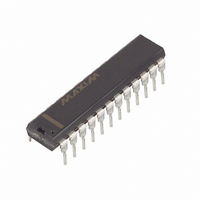
DS1742W-120+ Maxim Integrated Products, DS1742W-120+ Datasheet

DS1742W-120+
Specifications of DS1742W-120+
Related parts for DS1742W-120+
DS1742W-120+ Summary of contents
Page 1
... GND DQ3 ENCAPSULATED DIP PIN-PACKAGE TOP MARK** 24 EDIP (0.740a) DS1742-85 24 EDIP (0.740a) DS1742-85+ 24 EDIP (0.740a) DS1742-100 24 EDIP (0.740a) DS1742-100+ 24 EDIP (0.740a) DS1742-100IND 24 EDIP (0.740a) DS1742-100IND+ 24 EDIP (0.740a) DS1742W-120 24 EDIP (0.740a) DS1742W-120+ 24 EDIP (0.740a) DS1742W-150 24 EDIP (0.740a) DS1742W-150+ REV: 102808 RAM ...
Page 2
PIN DESCRIPTION PIN NAME Address Input A10 DQ0 10 DQ1 11 DQ2 13 DQ3 Data Input/Output 14 DQ4 ...
Page 3
CLOCK OPERATIONS—READING THE CLOCK While the double-buffered register structure reduces the chance of reading incorrect data, internal updates to the DS1742 clock registers should be halted before clock data is read to prevent reading of data in transition. However, halting ...
Page 4
SETTING THE CLOCK As shown in Table 2, bit 7 of the century register is the write bit. Setting the write bit like the read bit, halts updates to the DS1742 registers. The user can then load ...
Page 5
RETRIEVING DATA FROM RAM OR CLOCK The DS1742 is in the read mode wheneve high, and (chip enable) is low. The device architecture allows ripple-through access to any CE of the address locations in the NV SRAM. Valid data will ...
Page 6
BATTERY LONGEVITY The DS1742 has a lithium power source that is designed to provide energy for clock activity, and clock and RAM data retention when the V internal power supply is sufficient to power the DS1742 continuously for the life ...
Page 7
ABSOLUTE MAXIMUM RATINGS Voltage Range on Any Pin Relative to Ground……………………………………..-0.3V to +6.0V Storage Temperature Range………………………………………………………...-40°C to +85°C Soldering Temperature (EDIP, leads)..……………………..+260C for 10 seconds (See Note 7) This is a stress rating only and functional operation of the device ...
Page 8
DC ELECTRICAL CHARACTERISTICS = 3.3V 10%, Over the operating range PARAMETER Active Supply Current TTL Standby Current ( CMOS Standby Current 0.2V Input Leakage Current (any input) Output ...
Page 9
AC CHARACTERISTICS—READ CYCLE (3.3V) = 3.3V 10%, Over the operating range PARAMETER Read Cycle Time Address Access Time to DQ Low-Z CE Access Time CE Data Off time Low-Z OE Access Time OE Data Off ...
Page 10
AC CHARACTERISTICS—WRITE CYCLE (5V) = 5.0V 10%, Over the operating range PARAMETER SYMBOL Write Cycle Time Address Access Time Pulse Width WE Pulse Width CE Data Setup Time Data Hold time Address Hold Time Data Off Time WE ...
Page 11
WRITE CYCLE TIMING DIAGRAM—WRITE-ENABLE CONTROLLED WRITE CYCLE TIMING DIAGRAM—CHIP-ENABLE CONTROLLED DS1742 ...
Page 12
POWER-UP/POWER-DOWN CHARACTERISTICS (5V) = 5.0V 10%, Over the operating range PARAMETER Before Power-Down Fall Time PF(MAX) V Fall Time PF(MIN) V Rise ...
Page 13
POWER-UP/POWER-DOWN CHARACTERISTICS (3.3V) = 3.3V 10%, Over the operating range PARAMETER Before Power Down V Fall Time PF(MAX) V Rise Time PF(MIN) Power-Up ...
Page 14
AC TEST CONDITIONS Output Load: 100pF + 1TTL Gate Input Pulse Levels: 0.0 to 3.0V Timing Measurement Reference Levels: Input: 1.5V Output: 1.5V Input Pulse Rise and Fall Times: 5ns NOTES: 1) Voltage referenced to ground. 2) Typical values are ...
Page 15
PACKAGE INFORMATION For the latest package outline information and land patterns www.maxim-ic.com/packages. PACKAGE TYPE PACKAGE CODE 24 EDIP MDF24+1 DOCUMENT NO. 21-0245 ...
Page 16
... Maxim/Dallas Semiconductor cannot assume responsibility for use of any circuitry other than circuitry entirely embodied in a Maxim/Dallas Semiconductor product. No circuit patent licenses are implied. Maxim/Dallas Semiconductor reserves the right to change the circuitry and specifications without notice at any time The Maxim logo is a registered trademark of Maxim Integrated Products, Inc. The Dallas logo is a registered trademark of Dallas Semiconductor Corporation. DESCRIPTION © ...


