DS1747W-120+ Maxim Integrated Products, DS1747W-120+ Datasheet - Page 4
DS1747W-120+
Manufacturer Part Number
DS1747W-120+
Description
IC RTC RAM Y2K 3.3V 120NS 32EDIP
Manufacturer
Maxim Integrated Products
Type
Clock/Calendar/NVSRAM/Y2Kr
Datasheet
1.DS1747WP-120.pdf
(16 pages)
Specifications of DS1747W-120+
Memory Size
4M (512K x 8)
Time Format
HH:MM:SS (24 hr)
Date Format
YY-MM-DD-dd
Interface
Parallel
Voltage - Supply
3 V ~ 3.6 V
Operating Temperature
0°C ~ 70°C
Mounting Type
Through Hole
Package / Case
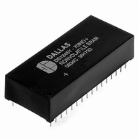
32-DIP Module (600 mil), 32-EDIP
Lead Free Status / RoHS Status
Lead free / RoHS Compliant


Figure 1. Block Diagram
PACKAGES
The DS1747 is available in two packages (32-pin DIP and 34-pin PowerCap module). The 32-pin DIP
style module integrates the crystal, lithium energy source, and silicon all in one package. The 34-pin
PowerCap Module Board is designed with contacts for connection to a separate PowerCap
(DS9034PCX) that contains the crystal and battery. This design allows the Power-Cap to be mounted on
top of the DS1747P after the completion of the surface mount process. Mounting the PowerCap after the
surface mount process prevents damage to the crystal and battery due to the high temperatures required
for solder reflow. The PowerCap is keyed to prevent reverse insertion. The PowerCap Module Board
and PowerCap are ordered separately and shipped in separate containers. The part number for the
PowerCap is DS9034PCX.
TIME AND DATE OPERATIONS
The contents of the time and date registers are in BCD format. The day-of-week register increments at
midnight. Values that correspond to the day of week are user-defined, but must be sequential (i.e., if 1
equals Sunday, then 2 equals Monday and so on). Illogical time and date entries result in undefined
operation.
CLOCK OPERATIONS—READING THE CLOCK
While the double-buffered register structure reduces the chance of reading incorrect data, internal
updates to the DS1747 clock registers should be halted before clock data is read to prevent reading of
data in transition. However, halting the internal clock register updating process does not affect clock
accuracy. Updating is halted when a one is written into the read bit, bit 6 of the century register (see
Table 2). As long as a one remains in that position, updating is halted. After a halt is issued, the registers
reflect the count, that is day, date, and time that was current at the moment the halt command was
issued. However, the internal clock registers of the double-buffered system continue to update so that
the clock accuracy is not affected by the access of data. All the DS1747 registers are updated
simultaneously after the internal clock register updating process has been re-enabled. Updating is within
a second after the read bit is written to zero. The READ bit must be set to a zero for a minimum of
500s to ensure the external registers will be updated.
DS1747/DS1747P Y2K-Compliant, Nonvolatile Timekeeping RAMs
DS1747
Maxim
4 of 16
Related parts for DS1747W-120+
Image
Part Number
Description
Manufacturer
Datasheet
Request
R

Part Number:
Description:
IC RTC RAM Y2K 3.3V 120NS 32EDIP
Manufacturer:
Maxim Integrated Products
Datasheet:
Part Number:
Description:
IC RTC RAM Y2K 3.3V 120NS 32EDIP
Manufacturer:
Maxim Integrated Products
Datasheet:
Part Number:
Description:
IC RTC RAM Y2K 3.3V 120NS 32EDIP
Manufacturer:
Maxim Integrated Products
Datasheet:

Part Number:
Description:
MAX7528KCWPMaxim Integrated Products [CMOS Dual 8-Bit Buffered Multiplying DACs]
Manufacturer:
Maxim Integrated Products
Datasheet:
Part Number:
Description:
Single +5V, fully integrated, 1.25Gbps laser diode driver.
Manufacturer:
Maxim Integrated Products
Datasheet:
Part Number:
Description:
Single +5V, fully integrated, 155Mbps laser diode driver.
Manufacturer:
Maxim Integrated Products
Datasheet:
Part Number:
Description:
VRD11/VRD10, K8 Rev F 2/3/4-Phase PWM Controllers with Integrated Dual MOSFET Drivers
Manufacturer:
Maxim Integrated Products
Datasheet:
Part Number:
Description:
Highly Integrated Level 2 SMBus Battery Chargers
Manufacturer:
Maxim Integrated Products
Datasheet:
Part Number:
Description:
Current Monitor and Accumulator with Integrated Sense Resistor; ; Temperature Range: -40°C to +85°C
Manufacturer:
Maxim Integrated Products
Part Number:
Description:
TSSOP 14/A°/RS-485 Transceivers with Integrated 100O/120O Termination Resis
Manufacturer:
Maxim Integrated Products
Part Number:
Description:
TSSOP 14/A°/RS-485 Transceivers with Integrated 100O/120O Termination Resis
Manufacturer:
Maxim Integrated Products
Part Number:
Description:
QFN 16/A°/AC-DC and DC-DC Peak-Current-Mode Converters with Integrated Step
Manufacturer:
Maxim Integrated Products
Part Number:
Description:
TDFN/A/65V, 1A, 600KHZ, SYNCHRONOUS STEP-DOWN REGULATOR WITH INTEGRATED SWI
Manufacturer:
Maxim Integrated Products
Part Number:
Description:
Integrated Temperature Controller f
Manufacturer:
Maxim Integrated Products
Part Number:
Description:
SOT23-6/I°/45MHz to 650MHz, Integrated IF VCOs with Differential Output
Manufacturer:
Maxim Integrated Products