DS1306EN Maxim Integrated Products, DS1306EN Datasheet - Page 11
DS1306EN
Manufacturer Part Number
DS1306EN
Description
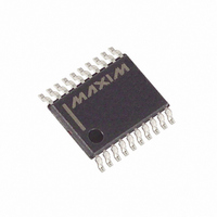
IC RTC SERIAL ALARM IND 20-TSSOP
Manufacturer
Maxim Integrated Products
Type
Clock/Calendar/Alarmr
Datasheet
1.DS1306E.pdf
(22 pages)
Specifications of DS1306EN
Memory Size
96B
Time Format
HH:MM:SS (12/24 hr)
Date Format
YY-MM-DD-dd
Interface
SPI, 3-Wire Serial
Voltage - Supply
2 V ~ 5.5 V
Operating Temperature
-40°C ~ 85°C
Mounting Type
Surface Mount
Package / Case
20-TSSOP
Lead Free Status / RoHS Status
Contains lead / RoHS non-compliant
Available stocks
Company
Part Number
Manufacturer
Quantity
Price

Part Number:
DS1306EN
Manufacturer:
MAXIM/ç¾ژن؟،
Quantity:
20 000
Company:
Part Number:
DS1306EN+
Manufacturer:
Maxim
Quantity:
3 844
Company:
Part Number:
DS1306EN+
Manufacturer:
AD
Quantity:
5 412
Part Number:
DS1306EN+
Manufacturer:
MAXIM/ç¾ژن؟،
Quantity:
20 000
Part Number:
DS1306EN+T
Manufacturer:
MAXIM/ç¾ژن؟،
Quantity:
20 000
Company:
Part Number:
DS1306EN+T&R
Manufacturer:
XILINX
Quantity:
210
Part Number:
DS1306EN+TR
Manufacturer:
MAXIM/ç¾ژن؟،
Quantity:
20 000


SERIAL INTERFACE
The DS1306 offers the flexibility to choose between two serial interface modes. The DS1306 can
communicate with the SPI interface or with a standard 3-wire interface. The interface method used is
determined by the SERMODE pin. When this pin is connected to V
When this pin is connected to ground, standard 3-wire communication is selected.
SERIAL PERIPHERAL INTERFACE (SPI)
The serial peripheral interface (SPI) is a synchronous bus for address and data transfer and is used when
interfacing with the SPI bus on specific Motorola microcontrollers such as the 68HC05C4 and the
68HC11A8. The SPI mode of serial communication is selected by tying the SERMODE pin to V
Four pins are used for the SPI. The four pins are the SDO (serial data out), SDI (serial data in), CE (chip
enable), and SCLK (serial clock). The DS1306 is the slave device in an SPI application, with the
microcontroller being the master.
The SDI and SDO pins are the serial data input and output pins for the DS1306, respectively. The CE
input is used to initiate and terminate a data transfer. The SCLK pin is used to synchronize data
movement between the master (microcontroller) and the slave (DS1306) devices.
The shift clock (SCLK), which is generated by the microcontroller, is active only during address and data
transfer to any device on the SPI bus. The inactive clock polarity is programmable in some
microcontrollers. The DS1306 determines on the clock polarity by sampling SCLK when CE becomes
active. Therefore either SCLK polarity can be accommodated. Input data (SDI) is latched on the internal
strobe edge and output data (SDO) is shifted out on the shift edge (Figure 5). There is one clock for each
bit transferred. Address and data bits are transferred in groups of eight, MSB first.
Figure 5. SERIAL CLOCK AS A FUNCTION OF MICROCONTROLLER
CLOCK POLARITY (CPOL)
CPOL = 0
CPOL = 1
NOTE 1: CPHA BIT POLARITY (IF APPLICABLE) MAY NEED TO BE SET ACCORDINGLY.
NOTE 2: CPOL IS A BIT THAT IS SET IN THE MICROCONTROLLER’S CONTROL REGISTER.
NOTE 3: SDO REMAINS AT HIGH-Z UNTIL 8 BITS OF DATA ARE READY TO BE SHIFTED OUT DURING A READ.
CE
SCLK
SCLK
SHIFT DATA OUT (READ)
SHIFT DATA OUT (READ)
11 of 22
CC
, SPI communication is selected.
DATA LATCH (WRITE)
DATA LATCH (WRITE)
CC
.
Related parts for DS1306EN
Image
Part Number
Description
Manufacturer
Datasheet
Request
R

Part Number:
Description:
IC RTC SERIAL ALARM 16-DIP
Manufacturer:
Maxim Integrated Products
Datasheet:
Part Number:
Description:
IC RTC SERIAL ALARM 16-DIP
Manufacturer:
Maxim Integrated Products
Datasheet:

Part Number:
Description:
Ds1306 Serial Alarm Real-time Clock
Manufacturer:
Maxim Integrated Products, Inc.
Datasheet:

Part Number:
Description:
MAX7528KCWPMaxim Integrated Products [CMOS Dual 8-Bit Buffered Multiplying DACs]
Manufacturer:
Maxim Integrated Products
Datasheet:
Part Number:
Description:
Single +5V, fully integrated, 1.25Gbps laser diode driver.
Manufacturer:
Maxim Integrated Products
Datasheet:
Part Number:
Description:
Single +5V, fully integrated, 155Mbps laser diode driver.
Manufacturer:
Maxim Integrated Products
Datasheet:
Part Number:
Description:
VRD11/VRD10, K8 Rev F 2/3/4-Phase PWM Controllers with Integrated Dual MOSFET Drivers
Manufacturer:
Maxim Integrated Products
Datasheet:
Part Number:
Description:
Highly Integrated Level 2 SMBus Battery Chargers
Manufacturer:
Maxim Integrated Products
Datasheet:
Part Number:
Description:
Current Monitor and Accumulator with Integrated Sense Resistor; ; Temperature Range: -40°C to +85°C
Manufacturer:
Maxim Integrated Products
Part Number:
Description:
TSSOP 14/A°/RS-485 Transceivers with Integrated 100O/120O Termination Resis
Manufacturer:
Maxim Integrated Products
Part Number:
Description:
TSSOP 14/A°/RS-485 Transceivers with Integrated 100O/120O Termination Resis
Manufacturer:
Maxim Integrated Products
Part Number:
Description:
QFN 16/A°/AC-DC and DC-DC Peak-Current-Mode Converters with Integrated Step
Manufacturer:
Maxim Integrated Products
Part Number:
Description:
TDFN/A/65V, 1A, 600KHZ, SYNCHRONOUS STEP-DOWN REGULATOR WITH INTEGRATED SWI
Manufacturer:
Maxim Integrated Products
Part Number:
Description:
Integrated Temperature Controller f
Manufacturer:
Maxim Integrated Products
Part Number:
Description:
SOT23-6/I°/45MHz to 650MHz, Integrated IF VCOs with Differential Output
Manufacturer:
Maxim Integrated Products