DS1284QN+ Maxim Integrated Products, DS1284QN+ Datasheet - Page 14
DS1284QN+
Manufacturer Part Number
DS1284QN+
Description
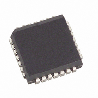
IC TIMEKEEPER WATCHDG IND 28PLCC
Manufacturer
Maxim Integrated Products
Type
Watchdog Timerr
Datasheet
1.DS1284QN.pdf
(18 pages)
Specifications of DS1284QN+
Memory Size
50B
Time Format
HH:MM:SS:hh (12/24 hr)
Date Format
YY-MM-DD-dd
Interface
Parallel
Voltage - Supply
4.5 V ~ 5.5 V
Operating Temperature
-40°C ~ 85°C
Mounting Type
Surface Mount
Package / Case
28-LCC, 28-PLCC
Lead Free Status / RoHS Status
Lead free / RoHS Compliant


NOTES:
1. WE is high for a read cycle.
2. OE = V
3. t
4. t
5. t
6. If the CE low transition occurs simultaneously with or later than the WE low transition in write cycle
7. If the CE high transition occurs prior to or simultaneously with the WE high transition, the output
8. If WE is low or the WE low transition occurs prior to or simultaneously with the CE low transition,
9. Each DS1284/DS1286 is marked with a four-digit date code AABB. AA designates the year of
10. All voltages are referenced to ground.
11. Applies to both interrupt pins when the alarms are set to pulse.
12. Interrupt output occurs within 100ns on the alarm condition existing.
13.
AC TEST CONDITIONS
Output Load: 100pF + 1TTL Gate
Input Pulse Levels: 0 to 3.0V
Timing Measurement Reference Levels
Input Pulse Rise and Fall Times: 5ns
PACKAGE INFORMATION
For the latest package outline information and land patterns, go to www.maxim-ic.com/packages.
PACKAGE TYPE
low to the earlier of CE or WE going high.
1, the output buffers remain in a high-impedance state during this period.
buffers remain in a high-impedance state during this period.
the output buffers remain in a high-impedance state during this period.
manufacture. BB designates the week of manufacture. The expected t
date of manufacture.
RTC modules can be successfully processed through conventional wave-soldering techniques as long
as temperature exposure to the lithium energy source contained within does not exceed +85°C.
However, post-solder cleaning with water-washing techniques is acceptable, provided that ultrasonic
vibrations are not used to prevent crystal damage.
WP
DS
DH
28 PLCC
28 PDIP
28 EDIP
or t
is measured from WE going high. If CE is used to terminate the write cycle, then t
Input: 1.5V
Output: 1.5V
is specified as the logical AND of CE and WE. t
DH
IH
are measured from the earlier of CE or WE going high.
or V
IL
. If OE = V
PACKAGE CODE
MDP28+1
Q28+11
P28+9
IH
during write cycle, the output buffers remain in a high-impedance state.
DOCUMENT NO.
21-0044
21-0049
21-0241
14 of 18
WP
is measured from the latter of CE or WE going
DR
is defined as starting at the
DH
DS1284/DS1286
= 20ns.
Related parts for DS1284QN+
Image
Part Number
Description
Manufacturer
Datasheet
Request
R

Part Number:
Description:
IC TIMEKEEPER WATCHDOG 28-DIP
Manufacturer:
Maxim Integrated Products
Datasheet:
Part Number:
Description:
IC TIMEKEEPER WATCHDOG 28-DIP
Manufacturer:
Maxim Integrated Products
Datasheet:

Part Number:
Description:
MAX7528KCWPMaxim Integrated Products [CMOS Dual 8-Bit Buffered Multiplying DACs]
Manufacturer:
Maxim Integrated Products
Datasheet:
Part Number:
Description:
Single +5V, fully integrated, 1.25Gbps laser diode driver.
Manufacturer:
Maxim Integrated Products
Datasheet:
Part Number:
Description:
Single +5V, fully integrated, 155Mbps laser diode driver.
Manufacturer:
Maxim Integrated Products
Datasheet:
Part Number:
Description:
VRD11/VRD10, K8 Rev F 2/3/4-Phase PWM Controllers with Integrated Dual MOSFET Drivers
Manufacturer:
Maxim Integrated Products
Datasheet:
Part Number:
Description:
Highly Integrated Level 2 SMBus Battery Chargers
Manufacturer:
Maxim Integrated Products
Datasheet:
Part Number:
Description:
Current Monitor and Accumulator with Integrated Sense Resistor; ; Temperature Range: -40°C to +85°C
Manufacturer:
Maxim Integrated Products
Part Number:
Description:
TSSOP 14/A°/RS-485 Transceivers with Integrated 100O/120O Termination Resis
Manufacturer:
Maxim Integrated Products
Part Number:
Description:
TSSOP 14/A°/RS-485 Transceivers with Integrated 100O/120O Termination Resis
Manufacturer:
Maxim Integrated Products
Part Number:
Description:
QFN 16/A°/AC-DC and DC-DC Peak-Current-Mode Converters with Integrated Step
Manufacturer:
Maxim Integrated Products
Part Number:
Description:
TDFN/A/65V, 1A, 600KHZ, SYNCHRONOUS STEP-DOWN REGULATOR WITH INTEGRATED SWI
Manufacturer:
Maxim Integrated Products
Part Number:
Description:
Integrated Temperature Controller f
Manufacturer:
Maxim Integrated Products
Part Number:
Description:
SOT23-6/I°/45MHz to 650MHz, Integrated IF VCOs with Differential Output
Manufacturer:
Maxim Integrated Products
Part Number:
Description:
SOT23-6/I°/45MHz to 650MHz, Integrated IF VCOs with Differential Output
Manufacturer:
Maxim Integrated Products