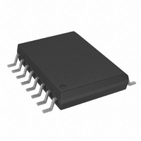
TC500ACOE Microchip Technology, TC500ACOE Datasheet - Page 9

TC500ACOE
Manufacturer Part Number
TC500ACOE
Description
IC ANALOG FRONT END 17BIT 16SOIC
Manufacturer
Microchip Technology
Specifications of TC500ACOE
Number Of Bits
17
Number Of Channels
1
Power (watts)
10mW
Voltage - Supply, Analog
5V
Voltage - Supply, Digital
4.5 V ~ 7.5 V
Package / Case
16-SOIC (0.300", 7.5mm Width)
Resolution (bits)
17bit
Sampling Rate
10SPS
Input Channel Type
Differential
Data Interface
3-Wire, Serial
Supply Voltage Range - Analog
± 4.5V To ± 7.5V
Supply Current
1mA
Lead Free Status / RoHS Status
Lead free / RoHS Compliant
Other names
158-1023
158-1023
158-1023
Available stocks
Company
Part Number
Manufacturer
Quantity
Price
Part Number:
TC500ACOE
Manufacturer:
MICROCHIP/微芯
Quantity:
20 000
4.0
4.1
Actual data conversion is accomplished in two
phases: input signal integration and reference voltage
de-integration.
The integrator output is initialized to 0V prior to the start
of integration. During integration, analog switch S
connects V
maintained for a fixed time period (T
application of V
0V at a rate determined by the magnitude of V
direction determined by the polarity of V
integration phase is initiated immediately at the
expiration of T
During de-integration, S1 connects a reference voltage
(having a polarity opposite that of V
input. At the same time, an external precision timer is
started. The de-integration phase is maintained until
the comparator output changes state, indicating the
integrator has returned to its starting point of 0V. When
this occurs, the precision timer is stopped. The de-
integration time period (T
precision timer, is directly proportional to the magnitude
of the applied input voltage (see
A simple mathematical equation relates the input
signal, reference voltage and integration time:
EQUATION 4-1:
For a constant V
EQUATION 4-2:
The dual slope converter accuracy is unrelated to the
integrating resistor and capacitor values as long as
they are stable during a measurement cycle.
An inherent benefit is noise immunity. Input noise
spikes are integrated (averaged to zero) during the
integration periods. Integrating ADCs are immune to
the large conversion errors that plague successive
approximation converters in high noise environments.
© 2008 Microchip Technology Inc.
Where:
t
DEINT
V
T
REF
INT
----------------------- -
R
INT
DETAILED DESCRIPTION
Dual Slope Conversion Principles
1
C
IN
=
=
=
INT
INT
IN
to the integrator input where it is
∫
Reference Voltage
Signal Integration time (fixed)
Reference Voltage Integration time
(variable)
IN
.
causes the integrator output to depart
T
0
V
:
INT
IN
V
=
IN
T ( )DT
V
DEINT
REF
T
----------------- -
DEINT
T
), as measured by the
=
INT
Figure
V
------------------------------- -
IN
REF
R
) to the integrator
INT
4-3).
C
C
DEINT
INT
IN
INT
. The de-
IN
). The
and a
1
Integrating converters provide inherent noise rejection
with at least a 20dB/decade attenuation rate.
Interference signals with frequencies at integral
multiples of the integration period are, theoretically,
completely removed, since the average value of a sine
wave of frequency (1/T) averaged over a period (T) is
zero.
Integrating converters often establish the integration
period to reject 50/60 Hz line frequency interference
signals. The ability to reject such signals is shown by a
normal mode rejection plot
rejection is limited in practice to 50 to 65 dB, since the
line frequency can deviate by a few tenths of a percent
(Figure
FIGURE 4-1:
Normal Mode Rejection.
FIGURE 4-2:
30
20
10
0.1/T
0
4-2).
Line Frequency Deviation from 60 Hz (%)
80
70
60
50
40
30
20
T = Measurment
0.01
TC500/A/510/514
Normal Mode = 20 LOG
Rejection
DEV = Deviation from 60 Hz
t = Integration Period
Period
Input Frequency
Integrating Converter
Line Frequency Deviation.
(Figure
0.1
1/T
t = 0.1 sec
SIN 60 t (1 –
60 t (1 –
4-1). Normal mode
p
p
DS21428E-page 9
DEV
DEV
100
100
)
)
1.0
10/T


