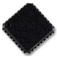
AD7195BCPZ Analog Devices Inc, AD7195BCPZ Datasheet - Page 25

AD7195BCPZ
Manufacturer Part Number
AD7195BCPZ
Description
IC AFE 24BIT 4.8K 32LFSP
Manufacturer
Analog Devices Inc
Datasheet
1.AD7195BCPZ-RL.pdf
(44 pages)
Specifications of AD7195BCPZ
Design Resources
Precision Weigh Scale Design Using AD7195 with Internal PGA and AC Excitation (CN0155)
Number Of Bits
24
Number Of Channels
4
Voltage - Supply, Analog
4.75 V ~ 5.25 V
Voltage - Supply, Digital
2.7 V ~ 5.25 V
Package / Case
32-LFCSP
Resolution (bits)
24bit
Sampling Rate
4.8kSPS
Input Channel Type
Pseudo Differential
Data Interface
3-Wire, Serial
Supply Voltage Range - Analog
4.75V To 5.25V
Lead Free Status / RoHS Status
Lead free / RoHS Compliant
Power (watts)
-
Lead Free Status / RoHS Status
Lead free / RoHS Compliant, Lead free / RoHS Compliant
Available stocks
Company
Part Number
Manufacturer
Quantity
Price
Company:
Part Number:
AD7195BCPZ
Manufacturer:
Analog Devices Inc
Quantity:
135
Company:
Part Number:
AD7195BCPZ
Manufacturer:
TST
Quantity:
5 000
Part Number:
AD7195BCPZ
Manufacturer:
ADI/亚德诺
Quantity:
20 000
Company:
Part Number:
AD7195BCPZ-RL
Manufacturer:
SEMTECH
Quantity:
394
ADC CIRCUIT INFORMATION
OVERVIEW
The AD7195 is an ultralow noise ADC that incorporates a Σ-Δ
modulator, a buffer, PGA, and on-chip digital filtering intended
for the measurement of wide dynamic range signals, such as
those in pressure transducers, weigh scales, and strain gage
applications. Figure 18 shows the block diagram for the part.
Analog Inputs
The device can be configured to have two differential or four
pseudo differential analog inputs. The analog inputs can be
buffered or unbuffered.
Multiplexer
The on-chip multiplexer increases the channel count of the
device. Because the multiplexer is included on chip, any
channel changes are synchronized with the conversion process.
PGA
The analog input signal can be amplified using the PGA. The
PGA allows gains of 1, 8, 16, 32, 64, and 128.
Reference Detect
The AD7195 is capable of monitoring the external reference. If
the reference is not present, a flag is set in the status register of
the device.
Burnout Currents
Two 500 nA burnout currents are included on-chip to detect
the presence of the external sensor.
AINCOM
BPDSW
AIN1
AIN2
AIN3
AIN4
AD7195
AV
DD
MUX
AGND
SENSOR
AGND
AV
TEMP
ACX1
DD
DV
DD
Figure 18. Block Diagram
Rev. 0 | Page 25 of 44
ACX1
DGND
PGA
EXCITATION
CLOCK
AC
REFIN(+) REFIN(–)
Σ-Δ ADC and Filter
The AD7195 contains a fourth-order Σ-Δ modulator followed
by a digital filter. The device offers the following filter options:
•
•
•
•
AC Excitation
The AD7195 supports ac excitation of load cells. It provides the
four logic outputs needed to control the transistors in an ac
excited load cell design.
Serial Interface
The AD7195 has a 4-wire SPI. The on-chip registers are
accessed via the serial interface.
Clock
The AD7195 has an internal 4.92 MHz clock. Either this clock
or an external clock can be used as the clock source to the
AD7195. The internal clock can also be made available on a
pin if a clock source is required for external circuitry.
Temperature Sensor
The on-chip temperature sensor monitors the die temperature.
Calibration
Both internal and system calibration are included on chip; thus,
the user has the option of removing offset/gain errors internal
to the AD7195 only, or removing the offset/gain errors of the
complete end system.
ACX2
ADC
Σ-Δ
Sinc
Sinc
Chop enabled/disabled
Zero latency
4
3
ACX2
INTERFACE
REFERENCE
CONTROL
MCLK1 MCLK2
SERIAL
DETECT
LOGIC
AND
CIRCUITRY
CLOCK
DOUT/RDY
DIN
SCLK
CS
SYNC
AD7195


