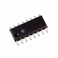
MCP3304-CI/SL Microchip Technology, MCP3304-CI/SL Datasheet - Page 21

MCP3304-CI/SL
Manufacturer Part Number
MCP3304-CI/SL
Description
IC ADC 13BIT 2.7V 4CH SPI 16SOIC
Manufacturer
Microchip Technology
Specifications of MCP3304-CI/SL
Package / Case
16-SOIC (0.154", 3.90mm Width)
Number Of Bits
13
Sampling Rate (per Second)
100k
Data Interface
Serial, SPI™
Number Of Converters
1
Voltage Supply Source
Single Supply
Operating Temperature
-40°C ~ 85°C
Mounting Type
Surface Mount
Architecture
SAR
Conversion Rate
100 KSPs
Resolution
12 bit
Input Type
Voltage
Snr
80.02 dB
Maximum Operating Temperature
+ 85 C
Mounting Style
SMD/SMT
Minimum Operating Temperature
- 40 C
Lead Free Status / RoHS Status
Lead free / RoHS Compliant
Lead Free Status / RoHS Status
Lead free / RoHS Compliant, Lead free / RoHS Compliant
Other names
MCP3304CI/SL
Available stocks
Company
Part Number
Manufacturer
Quantity
Price
Company:
Part Number:
MCP3304-CI/SL
Manufacturer:
MICROCHIP
Quantity:
12 000
Part Number:
MCP3304-CI/SL
Manufacturer:
MICROCHIP/微芯
Quantity:
20 000
Using an external operation amplifier on the input
allows for gain and also buffers the input signal from the
input to the ADC allowing for a higher source
impedance. This circuit is shown in
FIGURE 5-5:
for gain and also buffers the input from any high-
impedance sources.
This circuit shows that some headroom will be lost due
to the amplifier output not being able to swing all the
way to the rail. An example would be for an output
swing of 0V to 5V. This limitation can be overcome by
supplying a V
mode voltage. Using a 2.048V reference for the A/D
converter while biasing the input signal at 2.5V solves
the problem. This circuit is shown in
FIGURE 5-6:
amplifier output swing limitation.
© 2008 Microchip Technology Inc.
1 kΩ
1 kΩ
V
V
IN
IN
1 µF
1 µF
REF
10 kΩ
10 kΩ
MCP6021
MCP606
1 MΩ
1 MΩ
+
+
1 µF
-
-
1 µF
that is slightly less than the common
Adding an amplifier allows
Circuit solution to overcome
V
V
MCP1525
MCP1525
IN+
IN-
IN+
IN-
OUT
OUT
MCP330X
V
2.048V
MCP330X
V
REF
V
0.1 µF
Figure
0.1 µF
IN
Figure
IN
V
REF
V
V
0.1 µF
0.1 µF
DD
DD
5-5.
10 kΩ
5-5.
= 5V
= 5V
5.4
The common mode input range has no restriction and is
equal to the absolute input voltage range: V
V
mode voltage has a limited swing, if the entire range of
the A/D converter is to be used.
Figure 5-8
common mode voltage swing. A smaller V
wider flexibility in a common mode voltage. V
down to 400 mv, exhibit less than 0.1 LSB change in
DNL and INL. For characterization graphs that show
this performance relationship, see
Figure
FIGURE 5-7:
of Full Differential Input Signal versus V
FIGURE 5-8:
versus V
DD
-1
-1
5
4
3
2
1
0
0.25
+ 0.3V. However, for a given V
5
4
3
2
1
0
0.25
2-12.
Common Mode Input Range
REF
show the relationship between V
1.0
0.5
for Pseudo Differential Input.
MCP3302/04
Common Mode Input Range
Common Mode Input Range
V
V
REF
REF
2.5
1.25
4.05V
0.95V
4.05V
0.95V
(V)
(V)
DS21697E-page 21
REF
Figure 2-9
Figure 5-7
, the common
REF
4.0
2.0
V
V
REF
SS
DD
REF
REF
DD
allows for
-0.3V to
and the
= 5V
2.8V
2.3V
= 5V
2.8V
2.3V
.
levels,
5.0
2.5
and
and


