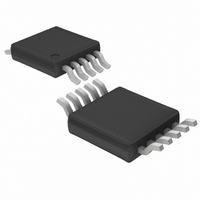
LTC2431CMS#PBF Linear Technology, LTC2431CMS#PBF Datasheet - Page 26

LTC2431CMS#PBF
Manufacturer Part Number
LTC2431CMS#PBF
Description
IC ADC 20BIT DIFFINPUT/REF10MSOP
Manufacturer
Linear Technology
Datasheet
1.LTC2431CMSPBF.pdf
(40 pages)
Specifications of LTC2431CMS#PBF
Number Of Bits
20
Sampling Rate (per Second)
7.5
Data Interface
MICROWIRE™, Serial, SPI™
Number Of Converters
2
Power Dissipation (max)
1mW
Voltage Supply Source
Single Supply
Operating Temperature
0°C ~ 70°C
Mounting Type
Surface Mount
Package / Case
10-TFSOP, 10-MSOP (0.118", 3.00mm Width)
Lead Free Status / RoHS Status
Lead free / RoHS Compliant
Available stocks
Company
Part Number
Manufacturer
Quantity
Price
APPLICATIO S I FOR ATIO
LTC2430/LTC2431
into about 0.11ppm additional INL error. When F
(internal oscillator and 50Hz notch), every 100 of source
resistance driving REF
0.092ppm additional INL error. When F
external oscillator with a frequency f
source resistance driving REF
about 0.73 • 10
ure 19 shows the typical INL error due to the source
resistance driving the REF
values are used. The effect of the source resistance on the
two reference pins is additive with respect to this INL error.
In general, matching of source impedance for the REF
26
Figure 18b. – FS Error vs R
Figure 18a. +FS Error vs R
–20
–30
–40
–50
–60
–10
60
50
40
30
20
10
0
0
0
0
V
V
V
V
V
F
T
V
V
V
V
V
F
T
C
O
O
CC
REF
REF
IN
IN
A
CC
REF
REF
IN
IN
A
100
100
REF
= GND
= 25 C
–6
= GND
= 25 C
+
–
+
–
= 5V
= 5V
+
–
= 1.25V
= 3.75V
+
–
= 3.75V
= 1.25V
= 1 F, 10 F
200
200
= 5V
= GND
= 5V
= GND
• f
U
300
300
EOSC
+
400
R
400
R
SOURCE
SOURCE
SOURCE
SOURCE
U
or REF
ppm additional INL error. Fig-
+
C
500
500
REF
or REF
= 1 F, 10 F
600
600
( )
( )
at REF
at REF
+
C
C
700
C
700
–
or REF
REF
C
REF
REF
REF
–
W
translates into about
= 0.01 F
800
pins when large C
800
= 0.01 F
+
= 0.1 F
+
EOSC
= 0.1 F
or REF
or REF
900
900
2431 F18b
2431 F18a
O
–
, every 100 of
1000
1000
is driven by an
translates into
–
–
(Large C
(Large C
U
O
= HIGH
REF
REF
REF
)
)
+
and REF
user is thus advised to minimize the combined source
impedance driving the REF
try to match it.
The magnitude of the dynamic reference current depends
upon the size of the very stable internal sampling capaci-
tors and upon the accuracy of the converter sampling
clock. The accuracy of the internal clock over the entire
temperature and power supply range is typical better than
1%. Such a specification can also be easily achieved by an
external clock. When relatively stable resistors (50ppm/ C)
are used for the external source impedance seen by REF
and REF
error will be insignificant (about 1% of its value over the
entire temperature and voltage range). Even for the most
stringent applications, a one-time calibration operation
may be sufficient.
In addition to the reference sampling charge, the reference
pins ESD protection diodes have a temperature dependent
leakage current. This leakage current, nominally 1nA
( 10nA max), results in a small gain error. A 100 source
resistance will create a 0.05 V typical and 0.5 V maxi-
mum full-scale error.
Figure 19. INL vs Differential Input Voltage (V
and Reference Source Resistance (R
for Large C
–
–
, the expected drift of the dynamic current gain
pins does not help the gain or the INL error. The
–12
–15
REF
–3
–6
–9
15
12
9
6
3
0
–0.5
V
V
V
V
Values (C
CC
REF
REF
INCM
–0.4
= 5V
+
–
= 5V
= GND
= 0.5(V
–0.3
–0.2
IN
REF
+
V
–0.1
+ V
INDIF
F
C
T
O
A
REF
IN
+
1 F)
= GND
= 25 C
/V
–
0
) = 2.5V
and REF
R
R
= 10 F
REFDIF
SOURCE
SOURCE
R
0.1 0.2
SOURCE
SOURCE
= 5k
= 10k
= 1k
0.3
–
pins rather than to
0.4
at REF
2431 F19
IN
0.5
= IN
+
+
and REF
– IN
–
)
24301f
–
)
+


