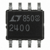
LTC2400CS8#PBF Linear Technology, LTC2400CS8#PBF Datasheet - Page 20

LTC2400CS8#PBF
Manufacturer Part Number
LTC2400CS8#PBF
Description
IC A/D CONV 24BIT MICRPWR 8-SOIC
Manufacturer
Linear Technology
Datasheet
1.LTC2400CS8PBF.pdf
(40 pages)
Specifications of LTC2400CS8#PBF
Number Of Bits
24
Sampling Rate (per Second)
7.5
Data Interface
MICROWIRE™, Serial, SPI™
Number Of Converters
1
Power Dissipation (max)
1mW
Voltage Supply Source
Single Supply
Operating Temperature
0°C ~ 70°C
Mounting Type
Surface Mount
Package / Case
8-SOIC (0.154", 3.90mm Width)
Lead Free Status / RoHS Status
Lead free / RoHS Compliant
Available stocks
Company
Part Number
Manufacturer
Quantity
Price
APPLICATIONS
LTC2400
During the conversion, the SCK and the serial data output
pin (SDO) are HIGH (EOC = 1). Once the conversion is
complete, SCK and SDO go LOW (EOC = 0) indicating the
conversion has finished and the device has entered the
low power sleep state. The part remains in the sleep state
a minimum amount of time (1/2 the internal SCK period)
then immediately begins outputting data. The data output
cycle begins on the first rising edge of SCK and ends after
the 32nd rising edge. Data is shifted out the SDO pin on
each falling edge of SCK. The internally generated serial
clock is output to the SCK pin. This signal may be used
to shift the conversion result into external circuitry. EOC
can be latched on the first rising edge of SCK and the last
bit of the conversion result can be latched on the 32nd
rising edge of SCK. After the 32nd rising edge, SDO goes
HIGH (EOC = 1) indicating a new conversion is in progress.
SCK remains HIGH during the conversion.
20
(INTERNAL)
GND
SDO
SCK
V
CS
CC
U
CONVERSION
INFORMATION
U
Hi-Z
W
Figure 11. Internal Serial Clock, Autostart Operation
–0.12V
SLEEP
REF
TO 1.12V
0.1V TO V
U
1 F
2.7V TO 5.5V
V
REF
V
REF
CC
IN
BIT 31
EOC
V
V
V
GND
CC
REF
IN
Internal Serial Clock, Autostart Conversion
This timing mode is identical to the internal serial clock,
2-wire I/O described above with one additional feature.
Instead of grounding CS, an external timing capacitor is
tied to CS.
While the conversion is in progress, the CS pin is held
HIGH by an internal weak pull-up. Once the conversion is
complete, the device enters the low power sleep state and
an internal 25nA current source begins discharging the
capacitor tied to CS, see Figure 11. The time the converter
spends in the sleep state is determined by the value of the
external timing capacitor, see Figures 12 and 13. Once the
voltage at CS falls below an internal threshold ( 1.4V), the
device automatically begins outputting data. The data
output cycle begins on the first rising edge of SCK and
ends on the 32nd rising edge. Data is shifted out the SDO
LTC2400
BIT 30
SDO
SCK
CS
F
O
DATA OUTPUT
BIT 29
SIG
C
EXT
V
CC
= 50Hz REJECTION
= EXTERNAL OSCILLATOR
= 60Hz REJECTION
BIT 0
CONVERSION
Hi-Z
2400 F11


