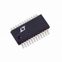
LTC1598LCG#PBF Linear Technology, LTC1598LCG#PBF Datasheet - Page 13

LTC1598LCG#PBF
Manufacturer Part Number
LTC1598LCG#PBF
Description
IC A/D CONV 12BIT SRL 8CH 24SSOP
Manufacturer
Linear Technology
Datasheet
1.LTC1598LCGPBF.pdf
(24 pages)
Specifications of LTC1598LCG#PBF
Number Of Bits
12
Sampling Rate (per Second)
10.5k
Data Interface
MICROWIRE™, QSPI™, Serial, SPI™
Number Of Converters
1
Power Dissipation (max)
480µW
Voltage Supply Source
Single Supply
Operating Temperature
0°C ~ 70°C
Mounting Type
Surface Mount
Package / Case
24-SSOP (0.200", 5.30mm Width)
Resolution (bits)
12bit
Sampling Rate
10.5kSPS
Input Channel Type
Single Ended
Supply Voltage Range - Analogue
2.7V To 3.6V
Supply Current
160µA
Rohs Compliant
Yes
Lead Free Status / RoHS Status
Lead free / RoHS Compliant
Available stocks
Company
Part Number
Manufacturer
Quantity
Price
APPLICATIONS
Operation with D
The LTC1594L/LTC1598L can be operated with D
D
required to communicate to the microprocessor (MPU).
Data is transmitted in both directions on a single wire.
The processor pin connected to this data line should be
configurable as either an input or an output. The
LTC1594L/LTC1598L will take control of the data line
after CS falling and before the 6th falling CLK while the
processor takes control of the data line when CS is high
COM = GND
DATA (D
OUT
MUXOUT
ADCIN =
CSMUX
CH0 TO
CSADC
D
CLK
CH7
OUT
D
IN
IN
/D
tied together. This eliminates one of the lines
CLK
OUT
CS
)
EN
D2
Hi-Z
D1
IN
U
D0
and D
t
SMPL
t
ON
INFORMATION
t
suCS
U
OUT
MPU CONTROLS DATA LINE AND SENDS
MUX ADDRESS TO LTC1594L/LTC1598L
NULL
Figure 3. LTC1594L/LTC1598L Operation with D
BIT
EN
1
B11
Tied Together
Figure 4. Selecting a Channel Once for Multiple Conversions
B10
W
B9
D2
2
DON’T CARE
B8
PROCESSOR MUST RELEASE DATA
B7
t
CONV
BEFORE THE 6TH FALLING CLK
B6
LINE AFTER CS FALLING AND
D1
B5
U
3
B4
IN
B3 B2
and
4
B1 B0
(see Figure 3). Therefore the processor port line must be
switched to an input with CS being low to avoid a conflict.
Separate Chip Selects for MUX and ADC
The LTC1594L/LTC1598L provide separate chip selects,
CSMUX and CSADC, to control MUX and ADC separately.
This feature not only provides the flexibility to select a
particular channel once for multiple conversions (see
Figure 4) but also maximizes the sample rate up to
20ksps (see Figure 5).
D0
D0
Hi-Z
t
SMPL
5
t
suCS
IN
t
NULL
suCS
BIT
and D
B11
B10
OUT
6
B9
Tied Together
DON’T CARE
LTC1594L/LTC1598L
B8
LTC1594L/LTC1598L CONTROLS DATA LINE AND SENDS
B7
t
CONV
LTC1594L/LTC1598L TAKES CONTROL OF DATA
LINE AFTER CS FALLING AND BEFORE THE
6TH FALLING CLK
B6
B5
A/D RESULT BACK TO MPU
B4
B11
B3 B2
B1 B0
B10
Hi-Z
13
1594L/98L F03
• • •
15948lfb
1594L/98L F04


