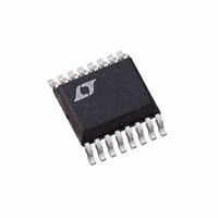
LTC1867ACGN#PBF Linear Technology, LTC1867ACGN#PBF Datasheet - Page 8

LTC1867ACGN#PBF
Manufacturer Part Number
LTC1867ACGN#PBF
Description
IC ADC 16BIT 8CH 200KSPS 16SSOP
Manufacturer
Linear Technology
Datasheet
1.LTC1867CGNPBF.pdf
(16 pages)
Specifications of LTC1867ACGN#PBF
Number Of Bits
16
Sampling Rate (per Second)
200k
Data Interface
MICROWIRE™, Serial, SPI™
Number Of Converters
1
Power Dissipation (max)
9mW
Voltage Supply Source
Single Supply
Operating Temperature
0°C ~ 70°C
Mounting Type
Surface Mount
Package / Case
16-SSOP (0.150", 3.90mm Width)
Number Of Elements
1
Resolution
16Bit
Architecture
SAR
Sample Rate
200KSPS
Input Polarity
Unipolar/Bipolar
Input Type
Voltage
Rated Input Volt
4.096/±2.048V
Differential Input
Yes
Power Supply Requirement
Analog and Digital
Single Supply Voltage (typ)
5V
Single Supply Voltage (min)
4.75V
Single Supply Voltage (max)
5.25V
Dual Supply Voltage (typ)
Not RequiredV
Dual Supply Voltage (min)
Not RequiredV
Dual Supply Voltage (max)
Not RequiredV
Power Dissipation
9mW
Differential Linearity Error
±1.75LSB
Integral Nonlinearity Error
±2.5LSB
Operating Temp Range
0C to 70C
Operating Temperature Classification
Commercial
Mounting
Surface Mount
Pin Count
16
Package Type
SSOP N
Lead Free Status / RoHS Status
Lead free / RoHS Compliant
Available stocks
Company
Part Number
Manufacturer
Quantity
Price
TIMING DIAGRAMS
LTC1863/LTC1867
CS/CONV
CS/CONV
CS/CONV
APPLICATIONS INFORMATION
Overview
The LTC1863/LTC1867 are complete, low power multi-
plexed ADCs. They consist of a 12-/16-bit, 200ksps capaci-
tive successive approximation A/D converter, a precision
internal reference, a confi gurable 8-channel analog input
multiplexer (MUX) and a serial port for data transfer.
Conversions are started by a rising edge on the CS/CONV
input. Once a conversion cycle has begun, it cannot be
restarted. Between conversions, the ADCs receive an input
word for channel selection and output the conversion
result, and the analog input is acquired in preparation for
the next conversion. In the acquire phase, a minimum time
of 1.5μs will provide enough time for the sample-and-hold
capacitors to acquire the analog signal.
8
SDO
SCK
Hi-Z
t
7
t
(SLEEP Mode Wake-Up Time)
50%
4
t 1
(SDO Valid After CONV↓)
(For Short Pulse Mode)
50%
SLEEP BIT (SLP = 0)
READ-IN
0.4V
t
1
t
4
t
7
50%
2.4V
0.4V
50%
CS/CONV
During the conversion, the internal differential 16-bit
capacitive DAC output is sequenced by the SAR from
the most signifi cant bit (MSB) to the least signifi cant bit
(LSB). The input is sucessively compared with the binary
weighted charges supplied by the differential capacitive
DAC. Bit decisions are made by a low-power, differential
comparator. At the end of a conversion, the DAC output
balances the analog input. The SAR contents (a 12-/16-bit
data word) that represent the analog input are loaded into
the 12-/16-bit output latches.
SDO
SCK
SDI
SDO
SCK
t
3
t
5
(SDO Valid Hold Time After SCK↓)
t
t
(SDI Setup Time Before SCK↑),
6
2.4V
0.4V
2
2.4V
t
(SDI Hold Time After SCK↑)
(SDO Valid Before SCK↑),
8
(BUS Relinquish Time)
t
8
t
5
90%
10%
2.4V
t
6
0.4V
2.4V
0.4V
t
t
3
2
Hi-Z
2.4V
0.4V
18637fa
1867 TD


