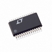
LTC1605-1CG#PBF Linear Technology, LTC1605-1CG#PBF Datasheet - Page 7

LTC1605-1CG#PBF
Manufacturer Part Number
LTC1605-1CG#PBF
Description
IC A/D CONV 16BIT SAMPLNG 28SSOP
Manufacturer
Linear Technology
Datasheet
1.LTC1605-1CGPBF.pdf
(20 pages)
Specifications of LTC1605-1CG#PBF
Number Of Bits
16
Sampling Rate (per Second)
100k
Data Interface
Parallel
Number Of Converters
1
Power Dissipation (max)
80mW
Voltage Supply Source
Analog and Digital
Operating Temperature
0°C ~ 70°C
Mounting Type
Surface Mount
Package / Case
28-SSOP (0.200", 5.30mm Width)
Lead Free Status / RoHS Status
Lead free / RoHS Compliant
Available stocks
Company
Part Number
Manufacturer
Quantity
Price
APPLICATIONS
TEST CIRCUITS
Conversion Details
The LTC1605-1/LTC1605-2 use a successive approxi-
mation algorithm and an internal sample-and-hold cir-
cuit to convert an analog signal to a 16-bit or two byte
parallel output. The ADC is complete with a precision
reference and an internal clock. The control logic pro-
vides easy interface to microprocessors and DSPs. (Please
refer to the Digital Interface section for the data format.)
Conversion start is controlled by the CS and R/C inputs.
At the start of conversion, the successive approximation
register (SAR) is reset. Once a conversion cycle has
begun, it cannot be restarted.
During the conversion, the internal 16-bit capacitive DAC
output is sequenced by the SAR from the most significant
bit (MSB) to the least significant bit (LSB). Referring to
Figure 1, V
and S1 to the sample-and-hold capacitor during the
acquire phase and the comparator offset is nulled by the
V
Figure 1. LTC1605-1/LTC1605-2 Simplified Equivalent Circuit
IN
DBN
R
A. HI-Z TO V
IN1
R
IN2
IN
1k
SAMPLE
is connected through the resistor divider
OH
HOLD
Load Circuit for Access Timing
S1
S2
AND V
U
OL
C
TO V
SAMPLE
C
V
DAC
DAC
INFORMATION
C
OH
U
L
DAC
B. HI-Z TO V
W
DBN
SAMPLE
–
+
COMPARATOR
OL
S3
AND V
5V
U
1k
C
OH
L
1605-1/2 TC01
1605-1/2 F01
LATCH
TO V
16-BIT
S
A
R
OL
autozero switch, S3. In this acquire phase, a minimum
delay of 2 s will provide enough time for the sample-and-
hold capacitor to acquire the analog signal. During the
convert phase, S3 opens, putting the comparator into the
compare mode. The input switch S2 switches C
ground, injecting the analog input charge onto the sum-
ming junction. This input charge is successively com-
pared with the binary-weighted charges supplied by the
capacitive DAC. Bit decisions are made by the high speed
comparator. At the end of a conversion, the DAC output
balances the V
bit data word) that represents the V
16-bit output latches.
Driving the Analog Inputs
The nominal input range for the LTC1605-1 is 0V to 4V or
(1.6V
or ( 1.6V
it should be driven by a low impedance source. Wideband
noise coupling into the input can be minimized by placing
a 1000pF capacitor at the input as shown in Figure 2. An
NPO-type capacitor gives the lowest distortion. Place the
capacitor as close to the device input pin as possible. If
an amplifier is to be used to drive the input, care should
be taken to select an amplifier with adequate accuracy,
linearity and noise for the application. The following list
is a summary of the op amps that are suitable for driving
the LTC1605-1/LTC1605-2. More detailed information is
available in the Linear Technology data books and
LinearView
LinearView is a trademark of Linear Technology Corporation
25V. The input impedance is typically 10k ; therefore,
DBN
REF
) and for the LTC1605-2 the input range is 4V
REF
TM
A. V
1k
Load Circuit for Output Float Delay
). The inputs are overvoltage protected to
CD-ROM.
IN
OH
LTC1605-1/LTC1605-2
TO HI-Z
input charge. The SAR contents (a 16-
50pF
DBN
IN
are loaded into the
B. V
OL
5V
TO HI-Z
1k
SAMPLE
50pF
1605-1/2 TC02
7
to


