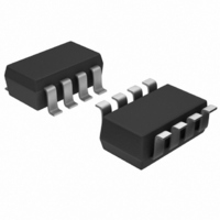
AD7999YRJZ-1500RL7 Analog Devices Inc, AD7999YRJZ-1500RL7 Datasheet - Page 24

AD7999YRJZ-1500RL7
Manufacturer Part Number
AD7999YRJZ-1500RL7
Description
IC ADC 8BIT 4CH SAR I2C SOT23-8
Manufacturer
Analog Devices Inc
Specifications of AD7999YRJZ-1500RL7
Data Interface
I²C, Serial
Design Resources
Using AD8599 as an Ultralow Distortion Driver for the AD7999 (CN0045)
Number Of Bits
8
Sampling Rate (per Second)
1M
Number Of Converters
1
Power Dissipation (max)
4.68mW
Voltage Supply Source
Single Supply
Operating Temperature
-40°C ~ 125°C
Mounting Type
Surface Mount
Package / Case
SOT-23-8
Resolution (bits)
8bit
Input Channel Type
Single Ended
Supply Voltage Range - Analogue
2.7V To 5.5V
Supply Current
850µA
No. Of Pins
8
Operating Temperature Range
-40°C To
Sampling Rate
140kSPS
Digital Ic Case Style
SOT-23
Rohs Compliant
Yes
Lead Free Status / RoHS Status
Lead free / RoHS Compliant
Other names
AD7999YRJZ-1500RL7TR
Available stocks
Company
Part Number
Manufacturer
Quantity
Price
Company:
Part Number:
AD7999YRJZ-1500RL7
Manufacturer:
ADI
Quantity:
3 000
Part Number:
AD7999YRJZ-1500RL7
Manufacturer:
ADI/亚德诺
Quantity:
20 000
AD7991/AD7995/AD7999
READING FROM THE AD7991/AD7995/AD7999
Reading data from the conversion result register is a 2-byte
operation, as shown in Figure 25. Therefore, a read operation
always involves two bytes.
After the AD7991/AD7995/AD7999 have received a read
address, any number of reads can be performed from the
conversion result register.
Following a start condition, the master writes the 7-bit address
of the AD7991/AD7995/AD7999 and then sets R/ W to 1. The
AD7991/AD7995/AD7999 acknowledge this by pulling the
SDA line low. They then output the conversion result over the
I
leading 0s followed by the channel identifier bits. For the
AD7995 there are two trailing 0s, and for the AD7999 there are
four trailing 0s.
After the master has addressed the AD7991/AD7995/AD7999,
the part begins to power up on the ninth SCLK rising edge. At
the same time, the acquisition phase begins. When approximately
0.6 μs have elapsed, the acquisition phase ends. The input is
sampled and a conversion begins. This is done in parallel to the
2
SDA
SCL
C bus, preceded by four status bits. The status bits are two
START BY
MASTER
0
1
1
SERIAL BUS ADDRESS BYTE
0
1
FRAME 1
Figure 25. Reading Two Bytes of Data from the AD7991Conversion Result Register
0
SCL (CONTINUED)
SDA (CONTINUED)
0
A0
R/W
ACK BY
Rev. 0 | Page 24 of 28
ADC
9
D7
1
0
1
read operation and should not affect the read operation. The
master reads back two bytes of data. On the ninth SCLK rising
edge of the second byte, if the master sends an ACK, it keeps
reading conversion results and the AD7991/AD7995/AD7999
powers up and performs a second conversion. If the master sends
a NO ACK, the AD7991/AD7995/AD7999 does not power up
on the ninth SCLK rising edge of the second byte. If a further
conversion is required, the part converts on the next channel, as
selected in the configuration register. See Table 11 for information
about the channel selection.
If the master sends a NO ACK on the ninth SCLK rising edge of
the second byte, the conversion is finished and no further
conversion is preformed.
To put the part into full shutdown mode, the user should issue a
stop condition to the AD7991/AD7995/AD7999. If the AD7991/
AD7995/AD7999 is not put into full shutdown mode, it will draw
a few tens of microamperes from the supply.
D6
LEAST SIGNIFICANT DATA BYTE FROM ADC
0
MOST SIGNIFICANT DATA BYTE FROM ADC
CH
D5
ID1
CH
D4
ID0
FRAME 2
FRAME 3
D11
D3
D10
D2
D1
D9
D8
D0
NO ACK BY
MASTER
MASTER
ACK BY
9
9
STOP BY
MASTER


