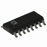
AD7888ARZ Analog Devices Inc, AD7888ARZ Datasheet - Page 11

AD7888ARZ
Manufacturer Part Number
AD7888ARZ
Description
IC ADC 12BIT 8CH SRL 16-SOIC
Manufacturer
Analog Devices Inc
Datasheet
1.AD7888ARZ.pdf
(17 pages)
Specifications of AD7888ARZ
Data Interface
DSP, MICROWIRE™, QSPI™, Serial, SPI™
Number Of Bits
12
Sampling Rate (per Second)
125k
Number Of Converters
1
Power Dissipation (max)
3.5mW
Voltage Supply Source
Single Supply
Operating Temperature
-40°C ~ 105°C
Mounting Type
Surface Mount
Package / Case
16-SOIC (0.154", 3.90mm Width)
Resolution (bits)
12bit
Sampling Rate
125kSPS
Input Channel Type
Single Ended
Supply Voltage Range - Analog
2.7V To 5.25V
Supply Current
700µA
Lead Free Status / RoHS Status
Lead free / RoHS Compliant
Available stocks
Company
Part Number
Manufacturer
Quantity
Price
Company:
Part Number:
AD7888ARZ
Manufacturer:
ADI
Quantity:
1 000
Part Number:
AD7888ARZ
Manufacturer:
ADI/亚德诺
Quantity:
20 000
Company:
Part Number:
AD7888ARZ-REEL7
Manufacturer:
ADI
Quantity:
1 000
REV. C
MODES OF OPERATION
The AD7888 has a number of different modes of operation.
These are designed to provide flexible power management
options. These options can be chosen to optimize the power
dissipation/throughput rate ratio for differing application require-
ments. The modes of operation are controlled by the PM1 and
PM0 bits of the Control Register as outlined previously.
Normal Mode (PM1 = 0, PM0 = 0)
This mode is intended for fastest throughput rate performance
as the user does not have to worry about any power-up times
with the AD7888 remaining fully powered all the time. Figure
13 shows the general diagram of the operation of the AD7888 in
this mode.
The data presented to the AD7888 on the DIN line during the
first eight clock cycles of the data transfer are loaded to the
Control Register. The part will remain powered up at the end of
the conversion as long as PM1 and PM0 were set to zero in the
write during that conversion. To continue to operate in this
mode, the user must ensure that PM1 and PM0 are both loaded
with 0 on every data transfer.
The falling edge of CS initiates the sequence and the input
signal is sampled on the second rising edge of the SCLK input.
Sixteen serial clock cycles are required to complete the conver-
sion and access the conversion result. Once a data transfer is
complete (CS has returned high), another conversion can be
initiated immediately by bringing CS low again.
DOUT
SCLK
DIN
CS
CONTROL REGISTER DATA IS LOADED ON THE
FIRST 8 CLOCKS. PM1 = 1 AND PM0 = 0
1
4 LEADING ZEROES + CONVERSION RESULT
DATA IN
CONVERSION AS PM1 = 1 AND PM0 = 0
SHUTDOWN AT THE END OF
SCLK
DOUT
DIN
CS
THE PART ENTERS
1
4 LEADING ZEROES + CONVERSION RESULT
DATA IN
CONTROL REGISTER DATA IS LOADED ON THE
FIRST 8 CLOCKS. PM1 AND PM0 = 0 TO KEEP
AT ALL TIMES AS PM1 AND PM0 = 0
THE PART REMAINS POWERED UP
16
THE PART IN THIS MODE
SHUTDOWN ON SCLK FALLING EDGE AS
Full Shutdown (PM1 = 0, PM0 = 1)
In this mode, all internal circuitry on the AD7888, including the
on-chip reference, is powered-down. The part retains the infor-
mation in the Control Register during full shutdown. The part
remains in full shutdown until the power management bits are
changed. If the power management bits are changed to PM1 = 1
and PM0 = 0, i.e., the autoshutdown mode, the part will remain
in shutdown (now in autoshutdown) but will power up once a
conversion is initiated after that (see Power-Up Times section).
The part changes mode as soon as the control register has been
updated, so if the part is in full shutdown mode and the power
management bits are changed to PM1 = PM0 = 0, i.e., normal
mode, then the part will power up on the 16th SCLK rising edge.
Autoshutdown (PM1 = 1, PM0 = 0)
In this mode, the AD7888 automatically enters its power-down
mode at the end of every conversion. Figure 14a shows the
general diagram of the operation of the AD7888 in this mode.
When CS goes from high to low, all on-chip circuitry will start
to power up on the next falling edge of SCLK. On the sixteenth
SCLK rising edge the part will power down again. It takes
approximately 5 µs for the AD7888 internal circuitry to be fully
powered up. As a result, a conversion (or sample-and-hold
acquisition) should not be initiated during this 5 µs. The input
signal is sampled on the second rising edge of SCLK following
the CS falling edge. The user should ensure that 5 µs elapse
between the first falling edge of SCLK after the falling edge of
THE PART POWERS UP FROM
PM1 = 1 AND PM0 = 0
PM1 = 1 AND PM0 = 0 TO KEEP THE
t
1
10
= 5 s
PART IN THIS MODE
2
4 LEADING ZEROES + CONVERSION RESULT
DATA IN
16
AD7888
16


