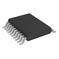
AD7866ARUZ Analog Devices Inc, AD7866ARUZ Datasheet - Page 12

AD7866ARUZ
Manufacturer Part Number
AD7866ARUZ
Description
IC ADC 12BIT 2CH DUAL 20-TSSOP
Manufacturer
Analog Devices Inc
Datasheet
1.AD7866ARU-REEL.pdf
(24 pages)
Specifications of AD7866ARUZ
Data Interface
DSP, MICROWIRE™, QSPI™, Serial, SPI™
Number Of Bits
12
Sampling Rate (per Second)
1M
Number Of Converters
2
Power Dissipation (max)
24mW
Voltage Supply Source
Analog and Digital
Operating Temperature
-40°C ~ 125°C
Mounting Type
Surface Mount
Package / Case
20-TSSOP (0.173", 4.40mm Width)
Resolution (bits)
12bit
Input Channel Type
Single Ended
Supply Voltage Range - Analogue
2.7V To 5.25V
Supply Voltage Range - Digital
2.7V To 5.25V
Supply
RoHS Compliant
Sampling Rate
1MSPS
Rohs Compliant
Yes
Number Of Elements
2
Resolution
12Bit
Architecture
SAR
Sample Rate
1MSPS
Input Polarity
Unipolar
Input Type
Voltage
Rated Input Volt
2.5/5V
Differential Input
No
Power Supply Requirement
Analog and Digital
Single Supply Voltage (typ)
3/5V
Single Supply Voltage (min)
2.7V
Single Supply Voltage (max)
5.25V
Dual Supply Voltage (typ)
Not RequiredV
Dual Supply Voltage (min)
Not RequiredV
Dual Supply Voltage (max)
Not RequiredV
Power Dissipation
24mW
Differential Linearity Error
-0.95LSB/1.25LSB
Integral Nonlinearity Error
±1.5LSB
Operating Temp Range
-40C to 125C
Operating Temperature Classification
Automotive
Mounting
Surface Mount
Pin Count
20
Package Type
TSSOP
Input Signal Type
Single-Ended
Lead Free Status / RoHS Status
Lead free / RoHS Compliant
For Use With
EVAL-AD7866CBZ - BOARD EVALUATION AD7866
Lead Free Status / Rohs Status
Compliant
Available stocks
Company
Part Number
Manufacturer
Quantity
Price
Part Number:
AD7866ARUZ
Manufacturer:
ADI/亚德诺
Quantity:
20 000
Part Number:
AD7866ARUZ-REEL7
Manufacturer:
ADI/亚德诺
Quantity:
20 000
AD7866
Analog Input Ranges
The analog input range for the AD7866 can be selected to be 0 V
to V
output coding. The RANGE pin is used to select both the analog
input range and the output coding, as shown in Figures 5 to 8.
On the falling edge of CS, point A, the logic level of the RANGE
pin is checked to determine the analog input range of the next
conversion. If this pin is tied to a logic low, the analog input
range will be 0 V to V
be straight binary (for the next conversion). If this pin is at a logic
high when CS goes low, the analog input range will be 2
the output coding for the part will be twos complement. How-
ever, if after the falling edge of CS, the logic level of the
RANGE pin has changed upon the eighth falling SCLK edge,
point B, the output coding will change to the other option without
any change in the analog input range. So for the next conversion,
twos complement output coding could be selected with a 0 V to
V
the falling edge of CS and high upon the eighth falling SCLK
edge, as shown in Figure 7. Figures 5 to 8 show examples of
timing diagrams for selections of different analog input ranges
with various output coding formats. Table I summarizes the
required logic level of the RANGE pin for each selection. Note
REF
REF
input range, for example, if the RANGE pin is low upon
or 2
V
REF
with either straight binary or twos complement
REF
Figure 6. Selecting V
RANGE
RANGE
D
D
D
D
SCLK
Figure 5. Selecting 0 V to V
SCLK
OUT
OUT
OUT
OUT
and the output coding from the part will
CS
CS
A
B
A
B
Range Level
Low
High
Low
High
NOTES
1
2
3
@ Point A
Point A = Falling edge of CS.
Point B = Eighth falling edge of SCLK.
Selected for next conversion.
1
A
A
Table I. Analog Input and Output Coding Selection
1
1
REF
Range Level
@ Point B
Low
High
High
Low
± V
REF
REF
B
B
V
Input Range with Twos Complement Output Coding
8
8
2
REF
Input Range with Straight Binary Output Coding
and
–12–
Input Range
0 V to V
V
V
0 V to 2
REF
REF
16
16
that the analog input range selected must not exceed V
logic input A0 is used to select the pair of channels to be converted
simultaneously. The logic state of this pin is also checked upon
the falling edge of CS, and the multiplexers are set up for the
next conversion. If it is low, the following conversion will be
performed on Channel 1 of each ADC; if it is high, the following
conversion will be performed on Channel 2 of each ADC.
Handling Bipolar Input Signals
Figure 9 shows how useful the combination of the 2
input range and the twos complement output coding scheme is
for handling bipolar input signals. If the bipolar input signal
is biased about V
selected, then V
negative full-scale, and +V
dynamic range of 2
Transfer Functions
The designed code transitions occur at successive integer LSB
values (i.e., 1 LSB, 2 LSB, and so on). The LSB size is V
The ideal transfer characteristic for the AD7866 when straight
binary coding is selected is shown in Figure 10, and the ideal
transfer characteristic for the AD7866 when twos complement
coding is selected is shown in Figure 11.
/2 ± V
± V
REF
INPUT RANGE
INPUT RANGE
0V TO V
V
REF
REF
V
REF
3
REF
V
REF
/2
REF
REF
REF
Output Coding
Straight Binary
Twos Complement
Twos Complement
Straight Binary
1
1
TWOS COMPLEMENT
becomes the zero code point, –V
STRAIGHT BINARY
and twos complement output coding is
V
REF
REF
.
becomes positive full-scale with a
16
16
3
REF
REF
DD
V
REV. A
REF
. The
/4096.
is


