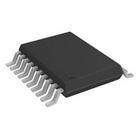
AD7328BRUZ Analog Devices Inc, AD7328BRUZ Datasheet - Page 6

AD7328BRUZ
Manufacturer Part Number
AD7328BRUZ
Description
IC ADC 12BIT+ SAR 8CHAN 20TSSOP
Manufacturer
Analog Devices Inc
Specifications of AD7328BRUZ
Data Interface
DSP, MICROWIRE™, QSPI™, Serial, SPI™
Design Resources
Using AD7328 in Appls with Single-Ended Industrial-Level Signals (CN0047)
Number Of Bits
12
Sampling Rate (per Second)
1M
Number Of Converters
1
Power Dissipation (max)
30mW
Voltage Supply Source
Dual ±
Operating Temperature
-40°C ~ 85°C
Mounting Type
Surface Mount
Package / Case
20-TSSOP (0.173", 4.40mm Width)
Resolution (bits)
13bit
Sampling Rate
1MSPS
Input Channel Type
Pseudo Differential, Single Ended
Supply Current
900µA
Digital Ic Case Style
TSSOP
No. Of Pins
20
Lead Free Status / RoHS Status
Lead free / RoHS Compliant
For Use With
EVAL-AD7328CBZ - BOARD EVALUATION FOR AD7328
Lead Free Status / Rohs Status
RoHS Compliant part
Electrostatic Device
Available stocks
Company
Part Number
Manufacturer
Quantity
Price
Part Number:
AD7328BRUZ
Manufacturer:
ADI/亚德诺
Quantity:
20 000
Company:
Part Number:
AD7328BRUZ-REEL7
Manufacturer:
ALLEGRO
Quantity:
1 200
AD7328
TIMING SPECIFICATIONS
V
T
Table 3.
Parameter
f
t
t
t
t
t
t
t
t
t
t
t
t
t
1
2
SCLK
CONVERT
QUIET
1
2
3
4
5
6
7
8
9
10
POWER-UP
Sample tested during initial release to ensure compliance. All input signals are specified with tr = tf = 5 ns (10% to 90% of V
When using the 0 V to 10 V unipolar range, running at 1 MSPS throughput rate with t at 20 ns, the mark space ratio needs to be limited to 50:50.
A
DD
2
= T
= 12 V to 16.5 V, V
MAX
to T
V
50
14
16 × t
75
12
25
45
26
57
0.4 × t
0.4 × t
13
40
10
4
2
750
500
25
MIN
CC
DOUT
SCLK
DIN
. Timing specifications apply with a 32 pF load, unless otherwise noted.
< 4.75 V
CS
SCLK
THREE-
SCLK
SCLK
STATE
SS
Limit at T
= −12 V to −16.5 V, V
WRITE
ADD2
t
2
1
3 IDENTIFICATION BITS
t
ADD1
3
50
14
750
25
V
20
16 × t
60
5
20
35
43
0.4 × t
0.4 × t
8
22
9
4
2
500
t
CC
SEL1
9
REG
MIN
= 4.75 V to 5.25 V
2
, T
SCLK
ADD0
SCLK
SCLK
MAX
SEL2
REG
3
SIGN
CC
MSB
= 2.7 V to 5.25 V, V
4
Figure 2. Serial Interface Timing Diagram
DB11
t
t
6
4
t
kHz min
MHz max
ns min
ns min
ns min
ns min
ns max
ns max
ns max
ns min
ns min
ns max
μs max
μs typ
Unit
ns max
ns min
ns min
ns min
ns min
CONVERT
t
10
5
t
DB10
7
Rev. A | Page 6 of 36
Description
V
t
Minimum time between end of serial read and next falling edge of CS
Minimum CS pulse width
CS to SCLK set-up time; bipolar input ranges (±10 V, ±5 V, ±2.5 V)
Unipolar input range (0 V to 10 V)
Delay from CS until DOUT three-state disabled
Data access time after SCLK falling edge
SCLK low pulse width
SCLK high pulse width
SCLK to data valid hold time
SCLK falling edge to DOUT high impedance
SCLK falling edge to DOUT high impedance
DIN set-up time prior to SCLK falling edge
DIN hold time after SCLK falling edge
Power up from autostandby
Power up from full shutdown/autoshutdown mode, internal reference
Power up from full shutdown/autoshutdown mode, external reference
DRIVE
SCLK
2
DRIVE
13
= 1/f
= 2.7 V to 5.25 V, V
DB2
≤ V
SCLK
CC
14
t
5
DB1
LSB
15
DB0
1
DON’T
CARE
16
REF
THREE-STATE
= 2.5 V to 3.0 V internal/external,
t
8
DRIVE
t
) and timed from a voltage level of 1.6 V.
QUIET
t
1


