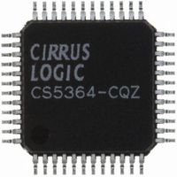
CS5364-CQZ Cirrus Logic Inc, CS5364-CQZ Datasheet - Page 21

CS5364-CQZ
Manufacturer Part Number
CS5364-CQZ
Description
IC ADC 4CH 114DB 216KHZ 48-LQFP
Manufacturer
Cirrus Logic Inc
Datasheet
1.CS5364-CQZ.pdf
(42 pages)
Specifications of CS5364-CQZ
Package / Case
48-LQFP
Number Of Converters
1
Number Of Bits
24
Sampling Rate (per Second)
216k
Data Interface
Serial
Power Dissipation (max)
580mW
Voltage Supply Source
Analog and Digital
Operating Temperature
-40°C ~ 85°C
Mounting Type
Surface Mount
Conversion Rate
192 KSPS
Resolution
24 bit
Number Of Adc Inputs
4
Operating Supply Voltage
5 V
Maximum Operating Temperature
+ 85 C
Minimum Operating Temperature
- 40 C
Mounting Style
SMD/SMT
Power Consumption
365 mW
Supply Voltage (max)
5.25 V
Supply Voltage (min)
4.75 V
Lead Free Status / RoHS Status
Lead free / RoHS Compliant
For Use With
CDB5364 - EVALUATION BOARD FOR CS5364
Lead Free Status / Rohs Status
Lead free / RoHS Compliant
Other names
598-1088
Available stocks
Company
Part Number
Manufacturer
Quantity
Price
Company:
Part Number:
CS5364-CQZ
Manufacturer:
CIRRUS
Quantity:
21
Company:
Part Number:
CS5364-CQZR
Manufacturer:
Cirrus Logic Inc
Quantity:
10 000
DS625F4
4.4
4.4.1 Synchronization of Multiple Devices
Master and Slave Operation
CS5364 operation depends on two clocks that are synchronously derived from MCLK: SCLK and LRCK/FS.
See
The CS5364 can operate as either clock master or clock slave with respect to SCLK and LRCK/FS. In Mas-
ter Mode, the CS5364 derives SCLK and LRCK/FS synchronously from MCLK and outputs the derived
clocks on the SCLK pin (pin 25) and the LRCK/FS pin (pin 24), respectively. In Slave Mode, the SCLK and
LRCK/FS are inputs, and the input signals must be synchronously derived from MCLK by a separate device
such as another CS5364 or a microcontroller.
both Master and Slave Modes.
The Master/Slave operation is controlled through the settings of M1 and M0 pins in Stand-Alone Mode or
by the M[1] and M[0] bits in the Global Mode Control Register in Control Port Mode. See
23
To ensure synchronous sampling in applications where multiple ADCs are used, the MCLK and LRCK must
be the same for all CS5364 devices in the system. If only one master clock source is needed, one solution
is to place one CS5364 in Master Mode, and slave all of the other devices to the one master, as illustrated
in
external source and time the CS5364 reset de-assertion with the falling edge of MCLK. This will ensure that
all converters begin sampling on the same clock edge.
Figure
for more information regarding the configuration of M1 and M0 pins or M[1] and M[0] bits.
Section 4.5 on page 22
9. If multiple master clock sources are needed, one solution is to supply all clocks from the same
Figure 9. Master and Slave Clocking for a Multi-Channel Application
Master
ADC as
master
clock
ADC
LRCK/FS
SCLK
for a detailed description of SCLK and LRCK/FS.
Figure 8. Master/Slave Clock Flow
SCLK & LRCK/FS
Controller
Figure 8
illustrates the clock flow of SCLK and LRCK/FS in
Slave1
Slave2
Slave3
ADC
ADC
ADC
ADC as
slave
clock
LRCK/FS
SCLK
Controller
Section 4.6 on page
CS5364
21


