ADC0838CCN/NOPB National Semiconductor, ADC0838CCN/NOPB Datasheet - Page 6
ADC0838CCN/NOPB
Manufacturer Part Number
ADC0838CCN/NOPB
Description
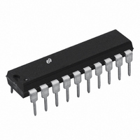
IC ADC 8BIT SERIAL I/O 20-DIP
Manufacturer
National Semiconductor
Datasheet
1.ADC0831CCWMNOPB.pdf
(33 pages)
Specifications of ADC0838CCN/NOPB
Number Of Bits
8
Sampling Rate (per Second)
31k
Data Interface
NSC MICROWIRE™, Serial
Number Of Converters
1
Power Dissipation (max)
15mW
Voltage Supply Source
Single Supply
Operating Temperature
0°C ~ 70°C
Mounting Type
Through Hole
Package / Case
20-DIP (0.300", 7.62mm)
Lead Free Status / RoHS Status
Lead free / RoHS Compliant
Other names
*ADC0838CCN
*ADC0838CCN/NOPB
ADC0838
ADC0838CCN
*ADC0838CCN/NOPB
ADC0838
ADC0838CCN


www.national.com
f
t
Clock Duty Cycle
(Note 10)
t
Data Input Valid to CLK
Rising Edge
t
after CLK Rising Edge
t
Edge to Output Data Valid
(Note 11)
t
CS to Data Output and
SARS Hi–Z
C
Input
C
Outputs
CLK
C
SET-UP
HOLD
pd1
1H
IN
OUT
, Conversion Time
AC Characteristics
The following specifications apply for V
Note 1: Absolute Maximum Ratings indicate limits beyond which damage to the device may occur. DC and AC electrical specifications do not apply when operating
the device beyond its specified operating conditions.
Note 2: All voltages are measured with respect to the ground plugs.
Note 3: Internal zener diodes (6.3 to 8.5V) are connected from V+ to GND and V
to V
is powered from V+. Functionality is therefore guaranteed for V+ operation even though the resultant voltage at V
It is recommended that a resistor be used to limit the max current into V+. (See Figure 3 in Functional Description Section 6.0)
Note 4: When the input voltage (V
to 5 mA or less. The 20 mA package input current limits the number of pins that can exceed the power supply boundaries with a 5 mA current limit to four.
Note 5: Human body model, 100 pF discharged through a 1.5 kΩ resistor.
Note 6: Total unadjusted error includes offset, full-scale, linearity, and multiplexer errors.
Note 7: Cannot be tested for ADC0832.
Note 8: For V
for analog input voltages one diode drop below ground or one diode drop greater than the V
level analog inputs (5V) can cause this input diode to conduct — especially at elevated temperatures, and cause errors for analog inputs near full-scale. The spec
allows 50 mV forward bias of either diode. This means that as long as the analog V
code will be correct. To achieve an absolute 0 V
variations, initial tolerance and loading.
Note 9: Leakage current is measured with the clock not switching.
Note 10: A 40% to 60% clock duty cycle range insures proper operation at all clock frequencies. In the case that an available clock has a duty cycle outside of these
limits, the minimum, time the clock is high or the minimum time the clock is low must be at least 1 µs. The maximum time the clock can be high is 60 µs. The clock
can be stopped when low so long as the analog input voltage remains stable.
Note 11: Since data, MSB first, is the output of the comparator used in the successive approximation loop, an additional delay is built in (see Block Diagram) to allow
for comparator response time.
Note 12: Typicals are at 25˚C and represent most likely parametric norm.
Note 13: Tested limits are guaranteed to National’s AOQL (Average Outgoing Quality Level).
Note 14: Guaranteed but not 100% production tested. These limits are not used to calculate outgoing quality levels.
, t
, Capacitance of Logic
, t
, Clock Frequency
0H
CC
, Capacitance of Logic
, Data Input Valid
pd0
, CS Falling Edge or
, — Rising Edge of
via a conventional diode. Since the zener voltage equals the A/D’s breakdown voltage, the diode insures that V
— CLK Falling
IN
Parameter
(−)≥V
IN
(+) the digital output code will be 0000 0000. Two on-chip diodes are tied to each analog input (see Block Diagram) which will forward conduct
IN
) at any pin exceeds the power supply rails (V
Min
Max
Min
Max
DC
Not including MUX Addressing Time
C
Data MSB First
Data LSB First
C
(see TRI-STATE
C
CC
L
L
L
to 5 V
=100 pF
=10 pF, R
=100 pf, R
= 5V, t
DC
input voltage range will therefore require a minimum supply voltage of 4.950 V
r
= t
L
L
Conditions
=10k
=2k
f
= 20 ns and 25˚C unless otherwise specified.
®
Test Circuits)
6
CC
IN
IN
to GND. The zener at V+ can operate as a shunt regulator and is connected
<
or V
V
−
REF
or V
CC
does not exceed the supply voltage by more than 50 mV, the output
IN
supply. Be careful, during testing at low V
>
V
+
(Note 12)
) the absolute value of current at that pin should be limited
Typ
650
250
125
5
5
CC
may exceed the specified Absolute Max of 6.5V.
CC
(Note 13)
will be below breakdown when the device
Tested
Limit
500
10
8
(Note 14)
CC
Design
Limit
1500
levels (4.5V), as high
400
250
600
250
DC
40
60
90
over temperature
1/f
Units
Limit
kHz
kHz
pF
pF
ns
ns
ns
ns
ns
ns
%
%
CLK
Related parts for ADC0838CCN/NOPB
Image
Part Number
Description
Manufacturer
Datasheet
Request
R

Part Number:
Description:
National Semiconductor [8-Bit D/A Converter]
Manufacturer:
National Semiconductor
Datasheet:
Part Number:
Description:
National Semiconductor [Media Coprocessor]
Manufacturer:
National Semiconductor
Datasheet:
Part Number:
Description:
Digitally Controlled Tone and Volume Circuit with Stereo Audio Power Amplifier, Microphone Preamp Stage and National 3D Sound
Manufacturer:
National Semiconductor
Datasheet:
Part Number:
Description:
Digitally Controlled Tone and Volume Circuit with Stereo Audio Power Amplifier, Microphone Preamp Stage and National 3D Sound
Manufacturer:
National Semiconductor
Datasheet:
Part Number:
Description:
AC97 Rev 2 Codec with Sample Rate Conversion and National 3D Sound
Manufacturer:
National Semiconductor
Part Number:
Description:
Manufacturer:
National Semiconductor
Datasheet:
Part Number:
Description:
Manufacturer:
National Semiconductor
Datasheet:
Part Number:
Description:
General Purpose, Low Voltage, Low Power, Rail-to-Rail Output Operational Amplifiers
Manufacturer:
National Semiconductor
Datasheet:
Part Number:
Description:
8-bit 20 MSPS flash A/D converter.
Manufacturer:
National Semiconductor
Datasheet:
Part Number:
Description:
Low Noise Quad Operational Amplifier
Manufacturer:
National Semiconductor
Datasheet:
Part Number:
Description:
Quad Differential Line Receivers
Manufacturer:
National Semiconductor
Datasheet:
Part Number:
Description:
Quad High Speed Trapezoidal? Bus Transceiver
Manufacturer:
National Semiconductor
Datasheet:
Part Number:
Description:
Dual Line Receiver
Manufacturer:
National Semiconductor
Datasheet:
Part Number:
Description:
TTL to 10k ECL Level Translator with Latch
Manufacturer:
National Semiconductor
Datasheet: