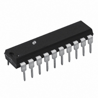
ADC0803LCN/NOPB National Semiconductor, ADC0803LCN/NOPB Datasheet - Page 16

ADC0803LCN/NOPB
Manufacturer Part Number
ADC0803LCN/NOPB
Description
IC ADC 8BIT MPU COMPAT 20-DIP
Manufacturer
National Semiconductor
Datasheet
1.ADC0803LCNNOPB.pdf
(41 pages)
Specifications of ADC0803LCN/NOPB
Number Of Bits
8
Number Of Converters
1
Power Dissipation (max)
875mW
Voltage Supply Source
Single Supply
Operating Temperature
-40°C ~ 85°C
Mounting Type
Through Hole
Package / Case
20-DIP (0.300", 7.62mm)
Number Of Elements
1
Resolution
8Bit
Architecture
SAR
Sample Rate
10KSPS
Input Polarity
Unipolar
Input Type
Voltage
Rated Input Volt
5V
Differential Input
Yes
Power Supply Requirement
Single
Single Supply Voltage (typ)
5V
Single Supply Voltage (min)
4.5V
Single Supply Voltage (max)
6.3V
Dual Supply Voltage (typ)
Not RequiredV
Dual Supply Voltage (min)
Not RequiredV
Dual Supply Voltage (max)
Not RequiredV
Power Dissipation
875mW
Operating Temp Range
-40C to 85C
Operating Temperature Classification
Industrial
Mounting
Through Hole
Pin Count
20
Package Type
PDIP
Input Signal Type
Differential
Lead Free Status / RoHS Status
Lead free / RoHS Compliant
Other names
*ADC0803LCN
www.national.com
Typical Applications
Note 11: Oversample whenever possible [keep fs
Note 12: Consider the amplitude errors which are introduced within the passband of the filter.
(Complete shutdown takes
*Use ADC0801, 02, 03 or 05 for lowest power consumption.
Note: Logic inputs can be driven to V
Buffer prevents data bus from overdriving output of A/D when in shutdown mode.
Functional Description
1.0 UNDERSTANDING A/D ERROR SPECS
A perfect A/D transfer characteristic (staircase waveform) is
shown in Figure 1 . The horizontal scale is analog input
voltage and the particular points labeled are in steps of 1
LSB (19.53 mV with 2.5V tied to the V
output codes that correspond to these inputs are shown as
30 seconds.)
CC
with A/D supply at zero volts.
(Continued)
REF
>
Power Savings by A/D and V
/2 pin). The digital
2f(−60)] to eliminate input frequency folding (aliasing) and to allow for the skirt response of the filter.
70% Power Savings by Clock Gating
Sampling an AC Input Signal
16
D−1, D, and D+1. For the perfect A/D, not only will
center-value (A−1, A, A+1, . . . . ) analog inputs produce
the correct output digital codes, but also each riser (the
transitions between adjacent output codes) will be located
±
are ideal and have no width. Correct digital output codes will
be provided for a range of analog input voltages that extend
1
⁄
2
REF
LSB away from each center-value. As shown, the risers
Shutdown
DS005671-78
DS005671-79
DS005671-80


