ADC78H89CIMT/NOPB National Semiconductor, ADC78H89CIMT/NOPB Datasheet - Page 13
ADC78H89CIMT/NOPB
Manufacturer Part Number
ADC78H89CIMT/NOPB
Description
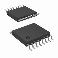
IC ADC 12BIT 500KSPS 7CH 16TSSOP
Manufacturer
National Semiconductor
Series
PowerWise®r
Datasheet
1.ADC78H89CIMTNOPB.pdf
(16 pages)
Specifications of ADC78H89CIMT/NOPB
Number Of Bits
12
Sampling Rate (per Second)
500k
Data Interface
DSP, MICROWIRE™, QSPI™, Serial, SPI™
Number Of Converters
1
Power Dissipation (max)
8.3mW
Voltage Supply Source
Analog and Digital
Operating Temperature
-40°C ~ 85°C
Mounting Type
Surface Mount
Package / Case
16-TSSOP (0.173", 4.40mm Width)
Number Of Elements
1
Resolution
12Bit
Architecture
SAR
Sample Rate
500KSPS
Input Polarity
Unipolar
Input Type
Voltage
Rated Input Volt
5.25V
Differential Input
No
Power Supply Requirement
Analog and Digital
Single Supply Voltage (typ)
3.3/5V
Single Supply Voltage (min)
2.7V
Single Supply Voltage (max)
5.25V
Dual Supply Voltage (typ)
Not RequiredV
Dual Supply Voltage (min)
Not RequiredV
Dual Supply Voltage (max)
Not RequiredV
Differential Linearity Error
±1LSB
Integral Nonlinearity Error
±1LSB
Operating Temp Range
-40C to 85C
Operating Temperature Classification
Industrial
Mounting
Surface Mount
Pin Count
16
Package Type
TSSOP
Input Signal Type
Single-Ended
Lead Free Status / RoHS Status
Lead free / RoHS Compliant
Other names
*ADC78H89CIMT
*ADC78H89CIMT/NOPB
ADC78H89CIMT
*ADC78H89CIMT/NOPB
ADC78H89CIMT
Available stocks
Company
Part Number
Manufacturer
Quantity
Price
Company:

Part Number:
ADC78H89CIMT/NOPB
Manufacturer:
TI
Quantity:
3 100


Applications Information
2.0 ADC78H89 OPERATION
The ADC78H89 is a successive-approximation analog-to-
digital converter designed around a charge-redistribution
digital-to-analog converter. Simplified schematics of the
ADC78H89 in both track and hold modes are shown in
Figure 2 and Figure 3, respectively. In Figure 2, the
ADD2
Bit 7 (MSB)
DONTC
0
0
0
0
1
1
1
1
Bit #:
7, 6, 2, 1, 0
5
4
3
TABLE 2. Input Channel Selection
ADD1
0
0
1
1
0
0
1
1
DONTC
Symbol:
DONTC
ADD2
ADD1
ADD0
Bit 6
ADD0
0
1
0
1
0
1
0
1
ADD2
Input Channel
Bit 5
Description
Don’t care. The value of this bit does not affect the device.
These three bits determine which input channel will be sampled and
converted on the next falling edge of CS. The mapping between codes and
channels is shown in Table 2.
AIN1 (Default)
FIGURE 2. ADC78H89 in Track Mode
(Continued)
FIGURE 3. ADC78H89 in Hold Mode
Control Register Bit Descriptions
AIN2
AIN3
AIN4
AIN5
AIN6
AIN7
GND
TABLE 1. Control Register Bits
ADD1
Bit 4
13
ADC78H89 is in track mode: switch SW1 connects the sam-
pling capacitor to one of seven analog input channels
through the multiplexer, and SW2 balances the comparator
inputs. The ADC78H89 is in this state for the first three SCLK
cycles after CS is brought low.
The user does not need to worry about any kind of power-up
delays or dummy conversions with the ADC78H89. The part
is able to acquire input to full resolution in the first conversion
immediately following power-up. The first conversion after
power up will be that of the first channel.
Figure 3 shows the ADC78H89 in hold mode: switch SW1
connects the sampling capacitor to ground, maintaining the
sampled voltage, and switch SW2 unbalances the compara-
tor. The control logic then instructs the charge-redistribution
DAC to add or subtract fixed amounts of charge from the
sampling capacitor until the comparator is balanced. When
the comparator is balanced, the digital word supplied to the
DAC is the digital representation of the analog input voltage.
The ADC78H89 is in this state for the last thirteen SCLK
cycles after CS is brought low.
ADD0
Bit 3
DONTC
Bit 2
20061609
20061610
DONTC
Bit 1
DONTC
www.national.com
Bit 0
Related parts for ADC78H89CIMT/NOPB
Image
Part Number
Description
Manufacturer
Datasheet
Request
R

Part Number:
Description:
National Semiconductor [8-Bit D/A Converter]
Manufacturer:
National Semiconductor
Datasheet:
Part Number:
Description:
National Semiconductor [Media Coprocessor]
Manufacturer:
National Semiconductor
Datasheet:
Part Number:
Description:
Digitally Controlled Tone and Volume Circuit with Stereo Audio Power Amplifier, Microphone Preamp Stage and National 3D Sound
Manufacturer:
National Semiconductor
Datasheet:
Part Number:
Description:
Digitally Controlled Tone and Volume Circuit with Stereo Audio Power Amplifier, Microphone Preamp Stage and National 3D Sound
Manufacturer:
National Semiconductor
Datasheet:
Part Number:
Description:
AC97 Rev 2 Codec with Sample Rate Conversion and National 3D Sound
Manufacturer:
National Semiconductor
Part Number:
Description:
Manufacturer:
National Semiconductor
Datasheet:
Part Number:
Description:
Manufacturer:
National Semiconductor
Datasheet:
Part Number:
Description:
General Purpose, Low Voltage, Low Power, Rail-to-Rail Output Operational Amplifiers
Manufacturer:
National Semiconductor
Datasheet:
Part Number:
Description:
8-bit 20 MSPS flash A/D converter.
Manufacturer:
National Semiconductor
Datasheet:
Part Number:
Description:
Low Noise Quad Operational Amplifier
Manufacturer:
National Semiconductor
Datasheet:
Part Number:
Description:
Quad Differential Line Receivers
Manufacturer:
National Semiconductor
Datasheet:
Part Number:
Description:
Quad High Speed Trapezoidal? Bus Transceiver
Manufacturer:
National Semiconductor
Datasheet:
Part Number:
Description:
Dual Line Receiver
Manufacturer:
National Semiconductor
Datasheet:
Part Number:
Description:
TTL to 10k ECL Level Translator with Latch
Manufacturer:
National Semiconductor
Datasheet: