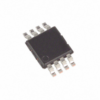
MAX11646EUA+ Maxim Integrated Products, MAX11646EUA+ Datasheet - Page 16

MAX11646EUA+
Manufacturer Part Number
MAX11646EUA+
Description
IC ADC 10BIT I2C 94.4KSPS 8UMAX
Manufacturer
Maxim Integrated Products
Datasheet
1.MAX11646EUA.pdf
(22 pages)
Specifications of MAX11646EUA+
Number Of Bits
10
Sampling Rate (per Second)
94.4k
Data Interface
I²C, Serial
Number Of Converters
1
Power Dissipation (max)
362mW
Voltage Supply Source
Single Supply
Operating Temperature
-40°C ~ 85°C
Mounting Type
Surface Mount
Package / Case
8-TSSOP, 8-MSOP (0.118", 3.00mm Width)
Number Of Adc Inputs
2
Conversion Rate
1 Ksps to 94.4 Ksps
Resolution
10 bit
Input Type
Single-Ended
Interface Type
I2C
Snr
60 dB
Voltage Reference
Internal 4.096 V
Supply Voltage (max)
5.5 V
Supply Voltage (min)
4.5 V
Maximum Power Dissipation
362 mW
Maximum Operating Temperature
+ 85 C
Input Voltage
4.5 V to 5.5 V
Minimum Operating Temperature
- 40 C
Lead Free Status / RoHS Status
Lead free / RoHS Compliant
Low-Power, 1-/2-Channel, I
in Ultra-Tiny 1.9mm x 2.2mm Package
When configured for internal clock mode (CLK = 0), the
MAX11646/MAX11647 use their internal oscillator as
the conversion clock. In internal clock mode, the
MAX11646/MAX11647 begin tracking the analog input
after a valid address on the eighth rising edge of the
clock. On the falling edge of the ninth clock, the analog
signal is acquired and the conversion begins. While
converting the analog input signal, the MAX11646/
MAX11647 hold SCL low (clock stretching). After the
conversion completes, the results are stored in internal
memory. If the scan mode is set for multiple conver-
sions, they all happen in succession with each addi-
tional result stored in memory. The MAX11646/
MAX11647 contain two 10-bit blocks of memory. Once
all conversions are complete, the MAX11646/MAX11647
release SCL, allowing it to be pulled high. The master can
now clock the results out of the memory in the same
Figure 10. Internal Clock Mode Read Cycles
16
A. SINGLE CONVERSION WITH INTERNAL CLOCK
B. SCAN MODE CONVERSIONS WITH INTERNAL CLOCK
1
S
1
S
SLAVE ADDRESS
______________________________________________________________________________________
SLAVE ADDRESS
MASTER TO SLAVE
SLAVE TO MASTER
7
t
ACQ
7
t
ACQ1
1 1
R
A
1 1
R
A
CLOCK STRETCH
t
CONV
t
CONV1
CLOCK STRETCH
RESULT 2 MSBs
t
ACQ2
t
CONV2
8
A
Internal Clock
CLOCK STRETCH
RESULT 8 LSBs
t
t
ACQN
CONVN
8
RESULT 1 ( 2MSBs)
1
A
P or Sr
8
1
order the scan conversion has been done at a clock
rate of up to 1.7MHz. SCL is stretched for a maximum
of 7.6µs per channel (see Figure 10).
The device memory contains all of the conversion results
when the MAX11646/MAX11647 release SCL. The con-
verted results are read back in a first-in/first-out (FIFO)
sequence. The memory contents can be read continu-
ously. If reading continues past the result stored in
memory, the pointer wraps around and point to the first
result. Note that only the current conversion results are
read from memory. The device must be addressed with
a read command to obtain new conversion results.
The internal clock mode’s clock stretching quiets the
SCL bus signal, reducing the system noise during con-
version. Using the internal clock also frees the bus
master (typically a microcontroller) from the burden of
running the conversion clock, allowing it to perform
other tasks that do not need to use the bus.
1
A
NUMBER OF BITS
RESULT 1 (8 LSBs) A
2
C, 10-Bit ADCs
8
1
RESULT N (8MSBs)
8
1
A
RESULT N (8LSBs)
8
1
A
P or Sr
1
NUMBER OF BITS


