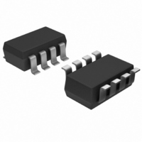
MAX11600EKA+T Maxim Integrated Products, MAX11600EKA+T Datasheet - Page 14

MAX11600EKA+T
Manufacturer Part Number
MAX11600EKA+T
Description
IC ADC SERIAL 8BIT 4CH SOT23-8
Manufacturer
Maxim Integrated Products
Datasheet
1.MAX11602EEE.pdf
(23 pages)
Specifications of MAX11600EKA+T
Number Of Bits
8
Sampling Rate (per Second)
188k
Data Interface
I²C, Serial
Number Of Converters
1
Power Dissipation (max)
1.75mW
Voltage Supply Source
Single Supply
Operating Temperature
-40°C ~ 85°C
Mounting Type
Surface Mount
Package / Case
SOT-23-8
Resolution
8 bit
Interface Type
I2C
Snr
49 dB
Voltage Reference
4.096 V
Supply Voltage (max)
5.5 V
Supply Voltage (min)
4.5 V
Maximum Power Dissipation
567 mW
Maximum Operating Temperature
+ 85 C
Mounting Style
SMD/SMT
Input Voltage
5 V
Minimum Operating Temperature
- 40 C
Lead Free Status / RoHS Status
Lead free / RoHS Compliant
Other names
MAX11600EKA+T
MAX11600EKA+TTR
MAX11600EKA+TTR
2.7V to 3.6V and 4.5V to 5.5V, Low-Power,
4-/8-/12-Channel 2-Wire Serial 8-Bit ADCs
random access memory (RAM). If the scan mode is set
for multiple conversions, they all happen in succession
with each additional result being stored in RAM. The
MAX11600/MAX11601 contain 8 bytes of RAM, the
MAX11602/MAX11603 contain 8 bytes of RAM, and the
MAX11604/MAX11605 contain 12 bytes of RAM. Once
all conversions are complete, the MAX11600–
MAX11605 release SCL, allowing it to be pulled high.
The master can now clock the results out of the output
shift register at a clock rate of up to 1.7MHz. SCL is
stretched for a maximum acquisition and conversion
time of 7.6µs per channel (Figure 10).
The device RAM contains all of the conversion results
when the MAX11600–MAX11605 release SCL. The con-
verted results are read back in a first-in-first-out (FIFO)
sequence. If AIN_/REF is set to be a reference input or
output (SEL1 = 1, Table 6), AIN_/REF is excluded from
a multichannel scan. This does not apply to the
MAX11602/MAX11603 as each provides separate pins
for AIN7 and REF. RAM contents can be read continu-
ously. If reading continues past the last result stored in
RAM, the pointer wraps around and points to the first
result. Note that only the current conversion results are
read from memory. The device must be addressed with
a read command to obtain new conversion results.
The internal clock mode’s clock stretching quiets the
SCL bus signal, reducing the system noise during con-
version. Using the internal clock also frees the master
(typically a microcontroller) from the burden of running
the conversion clock.
Figure 9. Write Cycle
14
______________________________________________________________________________________
A. 1-BYTE WRITE CYCLE
B. 2-BYTE WRITE CYCLE
1
S
1
S
SLAVE ADDRESS
SLAVE ADDRESS
MASTER TO SLAVE
SLAVE TO MASTER
7
7
SETUP OR CONFIGURATION BYTE
SETUP OR CONFIGURATION BYTE
MSB DETERMINES WHETHER
MSB DETERMINES WHETHER
W
W
1 1
1 1
A
A
CONFIGURATION BYTE
CONFIGURATION BYTE
SETUP OR
SETUP OR
8
8
A
A
1
1
When configured for external clock mode (CLK = 1),
the MAX11600–MAX11605 use SCL as the conversion
clock. In external clock mode, the MAX11600–
MAX11605 begin tracking the analog input on the sev-
enth falling clock edge of a valid slave address byte.
One SCL clock cycle later, the analog signal is
acquired and the conversion begins. Unlike internal
clock mode, converted data is available immediately
after the slave-address acknowledge bit. The device
continuously converts input channels dictated by the
scan mode until given a not acknowledge. There is no
need to re-address the device with a read command to
obtain new conversion results (Figure 11).
The conversion must complete in 9ms or droop on the
T/H capacitor degrades conversion results. Use internal
clock mode if the SCL clock period exceeds 1ms.
The MAX11600–MAX11605 must operate in external
clock mode for conversion rates up to 188ksps.
SCAN0 and SCAN1 of the configuration byte set the
scan-mode configuration. Table 5 shows the scanning
configurations. If AIN_/REF is set to be a reference input
or output (SEL1 = 1, Table 6), AIN_/REF is excluded
from a multichannel scan. This does not apply to the
MAX11602/MAX11603 as each provides separate pins
for AIN7 and REF.
P OR Sr
CONFIGURATION BYTE
1
SETUP OR
8
NUMBER OF BITS
A
1
P OR Sr
1
NUMBER OF BITS
External Clock
Scan Mode


