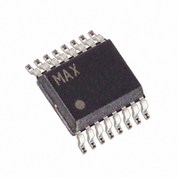
MAX1111EEE+ Maxim Integrated Products, MAX1111EEE+ Datasheet - Page 7

MAX1111EEE+
Manufacturer Part Number
MAX1111EEE+
Description
IC ADC 8BIT LP 16-QSOP
Manufacturer
Maxim Integrated Products
Datasheet
1.MAX1111CEE.pdf
(20 pages)
Specifications of MAX1111EEE+
Number Of Bits
8
Sampling Rate (per Second)
50k
Data Interface
MICROWIRE™, QSPI™, Serial, SPI™
Number Of Converters
1
Power Dissipation (max)
667mW
Voltage Supply Source
Single Supply
Operating Temperature
0°C ~ 70°C
Mounting Type
Surface Mount
Package / Case
16-SSOP (0.150", 3.90mm Width)
Number Of Adc Inputs
8
Architecture
SAR
Conversion Rate
50 KSPs
Resolution
8 bit
Input Type
Differential
Interface Type
4-Wire (SPI, QSPI, MICROWIRE)
Voltage Reference
Internal 2.048 V or External
Supply Voltage (max)
5 V
Maximum Power Dissipation
667 mW
Maximum Operating Temperature
+ 85 C
Mounting Style
SMD/SMT
Input Voltage
1.5 V
Minimum Operating Temperature
- 40 C
Lead Free Status / RoHS Status
Lead free / RoHS Compliant
Figure 1. Load Circuits for Enable Time
______________________________________________________________Pin Description
MAX1110
DOUT
1–4
5–8
a) High-Z to V
10
11
12
13
14
15
16
17
18
19
20
9
3k
PIN
OH
MAX1111
DGND
and V
1–4
10
11
12
13
14
15
16
—
5
6
7
8
9
_______________________________________________________________________________________
OL
to V
OH
C
LOAD
CH0–CH3
CH4–CH7
REFOUT
SSTRB
NAME
AGND
DGND
SHDN
REFIN
DOUT
SCLK
COM
V
DIN
CS
DD
b) High-Z to V
DOUT
+2.7V, Low-Power, Multichannel,
Sampling Analog Inputs
Sampling Analog Inputs
Ground Reference for Analog Inputs. Sets zero-code voltage in single-ended mode.
Must be stable to ±0.5 LSB.
Three-Level Shutdown Input. Normally floats. Pulling SHDN low shuts the MAX1110/
MAX1111 down to 10µA (max) supply current; otherwise, the devices are fully opera-
tional. Pulling SHDN high shuts down the internal reference.
Reference Voltage Input for Analog-to-Digital Conversion. Connect to REFOUT to use
the internal reference.
Internal Reference Generator Output. Bypass with a 1µF capacitor to AGND.
Analog Ground
Digital Ground
Serial-Data Output. Data is clocked out on SCLK’s falling edge. High impedance when
CS is high.
Serial-Strobe Output. In internal clock mode, SSTRB goes low when the MAX1110/
MAX1111 begin the A/D conversion and goes high when the conversion is done.
In external clock mode, SSTRB pulses high for two clock periods before the MSB is
shifted out. High impedance when CS is high (external clock mode only).
Serial-Data Input. Data is clocked in at SCLK’s rising edge. The voltage at DIN may
exceed V
Active-Low Chip Select. Data is not clocked into DIN unless CS is low. When CS is
high, DOUT is high impedance. The voltage at CS may exceed V
Serial-Clock Input. Clocks data in and out of serial interface. In external clock mode,
SCLK also sets the conversion speed (duty cycle must be 45% to 55%). The voltage at
SCLK may exceed V
Positive Supply Voltage, +2.7V to +5.5V
+3V
OL
and V
3k
C
DGND
LOAD
OH
DD
to V
(up to 5.5V).
OL
DD
(up to 5.5V).
Figure 2. Load Circuits for Disable Time
DOUT
3k
FUNCTION
Serial 8-Bit ADCs
a) V
DGND
OH
to High-Z
C
LOAD
DOUT
DD
b) V
(up to 5.5V).
OL
+3V
to High-Z
3k
C
DGND
LOAD
7


