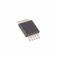
MAX1361EUB+ Maxim Integrated Products, MAX1361EUB+ Datasheet - Page 6

MAX1361EUB+
Manufacturer Part Number
MAX1361EUB+
Description
IC SYSTEM MON 10BIT 4CH 10-UMAX
Manufacturer
Maxim Integrated Products
Datasheet
1.MAX1361EUB.pdf
(24 pages)
Specifications of MAX1361EUB+
Number Of Bits
10
Sampling Rate (per Second)
150k
Data Interface
I²C, Serial
Number Of Converters
1
Power Dissipation (max)
2mW
Voltage Supply Source
Single Supply
Operating Temperature
-40°C ~ 85°C
Mounting Type
Surface Mount
Package / Case
10-MSOP, Micro10™, 10-uMAX, 10-uSOP
Number Of Adc Inputs
4
Architecture
SAR
Conversion Rate
150 KSPs
Resolution
10 bit
Interface Type
Serial (2-Wire, I2C, SMBus)
Voltage Reference
Internal 4.096 V or External
Supply Voltage (max)
3.3 V
Mounting Style
SMD/SMT
Lead Free Status / RoHS Status
Lead free / RoHS Compliant
4-Channel, 10-Bit, System Monitor with Programmable
Trip Window and SMBus Alert Response
ELECTRICAL CHARACTERISTICS (continued)
(V
0.1µF, f
Note 1: Devices configured for unipolar single-ended inputs.
Note 2: Relative accuracy is the deviation of the analog value at any code from its theoretical value after the gain and offset have
Note 3: Offset nulled.
Note 4: Conversion time is defined as the number of clock cycles needed for conversion multiplied by the clock period.
Note 5: The throughput rate of the I
Note 6: A filter on the SDA and SCL inputs suppresses noise spikes and delays the sampling instant.
Note 7: The absolute input voltage range for the analog inputs (AIN0–AIN3) is from GND to V
Note 8: When the internal reference is configured to be available at AIN3/REF (SEL[2:1] = 11), decouple AIN3/REF to GND with a
Note 9: ADC performance is limited by the converter’s noise floor, typically 300µV
Note 10: Maximum conversion throughput in internal clock mode when the data is not clocked out.
Note 11: For the MAX1361, PSRR is measured as
Note 12: C
Note 13: f
Note 14: A master device must provide a data hold time for SDA (referred to V
(V
T
6
A
DD
DD
-0.1
-0.2
-0.3
= +25°C, unless otherwise noted.)
0.3
0.2
0.1
_______________________________________________________________________________________
0
= 2.7V to 3.6V (MAX1361), V
= 3.3V (MAX1361), V
0
SCL
been calibrated.
Conversion time does not include acquisition time. SCL is the conversion clock in the external clock mode.
in monitor mode when not reading back results on the I
0.01µF capacitor.
and for the MAX1362, PSRR is measured as
falling edge.
SCLH
DIFFERENTIAL NONLINEARITY
= 1.7MHz, T
B
200
= total capacitance of one bus line in pF.
DIGITAL OUTPUT CODE
must meet the minimum clock low time plus the rise/fall times.
vs. DIGITAL CODE
⎡
⎢
⎢
⎣
⎡
⎢
⎢
⎣
400
⎡ ⎣
⎡ ⎣
V
V
FS
FS
( .
( .
A
600
5 5
3 6
= T
V
V
( .
( .
)
)
DD
MIN
3
5
−
−
800
5 5
6 6
V
V
V
V
FS
FS
= 5V (MAX1362), f
to T
− .
− .
( .
( .
1000
4 5
DD
2 7
4 5
2 7
MAX
2
C bus is limited to 94.4ksps. The MAX1361/MAX1362 can perform conversions up to 150ksps
V
V
V
V
= 4.5V to 5.5V (MAX1362), V
)
)
)
)
⎤ ⎦ ×
, unless otherwise noted. Typical values are at T
⎤ ⎦ ×
2
2
V
V
N
N
REF
REF
−
−
-0.1
-0.2
-0.3
-0.4
-0.5
1
1
0.5
0.4
0.3
0.2
0.1
⎤
⎥
⎥
⎦
0
⎤
⎥
⎥
⎦
0
SCL
= 1.7MHz, external clock, f
200
INTEGRAL NONLINEARITY
DIGITAL OUTPUT CODE
vs. DIGITAL CODE
400
2
C bus.
REF
600
Typical Operating Characteristics
= 2.048V (MAX1361), V
800
IL
of SCL) to bridge the undefined region of SCL’s
1000
P-P
.
SAMPLE
A
= +25°C.)
-100
-120
-140
-160
-20
-40
-60
-80
DD
= 94.4ksps, single-ended, unipolar,
0
0
.
REF
= 4.096V (MAX1362), C
10
FREQUENCY (kHz)
FFT PLOT
20
f
f
SAMPLE
IN
30
= 10kHz
= 94.4ksps
40
REF
50
=


