MAX1077ETC+ Maxim Integrated Products, MAX1077ETC+ Datasheet - Page 13
MAX1077ETC+
Manufacturer Part Number
MAX1077ETC+
Description
IC ADC 10BIT 1.5MSPS 12-TQFN
Manufacturer
Maxim Integrated Products
Datasheet
1.MAX1077ETC.pdf
(18 pages)
Specifications of MAX1077ETC+
Number Of Bits
10
Sampling Rate (per Second)
1.5M
Data Interface
MICROWIRE™, QSPI™, Serial, SPI™
Number Of Converters
1
Power Dissipation (max)
22mW
Voltage Supply Source
Analog and Digital
Operating Temperature
-40°C ~ 85°C
Mounting Type
Surface Mount
Package / Case
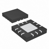
12-WQFN Exposed Pad
Number Of Adc Inputs
1
Architecture
SAR
Conversion Rate
1500 KSPs
Resolution
10 bit
Input Type
Differential
Interface Type
3-Wire (SPI, QSPI, MICROWIRE)
Voltage Reference
Internal 2.048 V or External
Supply Voltage (max)
3.6 V
Supply Voltage (min)
2.7 V
Maximum Power Dissipation
1349 mW
Maximum Operating Temperature
+ 85 C
Mounting Style
SMD/SMT
Minimum Operating Temperature
- 40 C
Lead Free Status / RoHS Status
Lead free / RoHS Compliant


remains valid until t
edge. When using CPOL = 0 and CPHA = 0 or CPOL = 1
and CPHA = 1, the data is clocked into the µP on the
following rising edge. When using CPOL = 0 and CPHA
= 1 or CPOL = 1 and CPHA = 0, the data is clocked
into the µP on the next falling edge. See Figure 11 for
connections and Figures 12 and 13 for timing. See the
Timing Characteristics section to determine the best
mode to use.
Unlike SPI, which requires two 1-byte reads to acquire
the 10 bits of data from the ADC, QSPI allows the mini-
mum number of clock cycles necessary to clock in the
Figure 12. SPI/MICROWIRE Serial-Interface Timing—Single Conversion (CPOL = CPHA = 0), (CPOL = CPHA = 1)
Figure 13. SPI/MICROWIRE Serial-Interface Timing—Continuous Conversion (CPOL = CPHA = 0), (CPOL = CPHA = 1)
Figure 14. QSPI Serial-Interface Timing—Single Conversion (CPOL = 1, CPHA = 1)
Differential, 10-Bit ADCs with Internal Reference
CNVST
DOUT
SCLK
CNVST
DOUT
SCLK
HIGH-Z
CNVST
DOUT
SCLK
1
1.5Msps, Single-Supply, Low-Power, True-
HIGH-Z
______________________________________________________________________________________
DHOLD
1
0
0
after the following SCLK rising
2
0
D9
D9
D8
D9
D8
D7
D8
D7
QSPI
D7
D6
D6
8
D6
D5
D5
D5
data. The MAX1077/MAX1079 require 16 clock cycles
from the µP to clock out the 10 bits of data. Figure 14
shows a transfer using CPOL = 1 and CPHA = 1. The
conversion result contains three zeros, followed by the
10 data bits, 2 sub-bits, and a trailing zero with the data
in MSB-first format.
The MAX1077/MAX1079 can be directly connected
to the TMS320C54_ family of DSPs from Texas
Instruments, Inc. Set the DSP to generate its own
clocks or use external clock signals. Use either the
standard or buffered serial port. Figure 15 shows the
simplest interface between the MAX1077/MAX1079 and
D4
9
D4
D4
D3
D3
D3
D2
DSP Interface to the TMS320C54_
D2
D2
D1
D1
D1
D0
S1
D0
D0
14
S0
S1
S1
16
HIGH-Z
S0
S0
16
16
0
HIGH-Z
1
0
13
Related parts for MAX1077ETC+
Image
Part Number
Description
Manufacturer
Datasheet
Request
R

Part Number:
Description:
MAX7528KCWPMaxim Integrated Products [CMOS Dual 8-Bit Buffered Multiplying DACs]
Manufacturer:
Maxim Integrated Products
Datasheet:
Part Number:
Description:
Single +5V, fully integrated, 1.25Gbps laser diode driver.
Manufacturer:
Maxim Integrated Products
Datasheet:
Part Number:
Description:
Single +5V, fully integrated, 155Mbps laser diode driver.
Manufacturer:
Maxim Integrated Products
Datasheet:
Part Number:
Description:
VRD11/VRD10, K8 Rev F 2/3/4-Phase PWM Controllers with Integrated Dual MOSFET Drivers
Manufacturer:
Maxim Integrated Products
Datasheet:
Part Number:
Description:
Highly Integrated Level 2 SMBus Battery Chargers
Manufacturer:
Maxim Integrated Products
Datasheet:
Part Number:
Description:
Current Monitor and Accumulator with Integrated Sense Resistor; ; Temperature Range: -40°C to +85°C
Manufacturer:
Maxim Integrated Products
Part Number:
Description:
TSSOP 14/A�/RS-485 Transceivers with Integrated 100O/120O Termination Resis
Manufacturer:
Maxim Integrated Products
Part Number:
Description:
TSSOP 14/A�/RS-485 Transceivers with Integrated 100O/120O Termination Resis
Manufacturer:
Maxim Integrated Products
Part Number:
Description:
QFN 16/A�/AC-DC and DC-DC Peak-Current-Mode Converters with Integrated Step
Manufacturer:
Maxim Integrated Products
Part Number:
Description:
TDFN/A/65V, 1A, 600KHZ, SYNCHRONOUS STEP-DOWN REGULATOR WITH INTEGRATED SWI
Manufacturer:
Maxim Integrated Products
Part Number:
Description:
Integrated Temperature Controller f
Manufacturer:
Maxim Integrated Products
Part Number:
Description:
SOT23-6/I�/45MHz to 650MHz, Integrated IF VCOs with Differential Output
Manufacturer:
Maxim Integrated Products
Part Number:
Description:
SOT23-6/I�/45MHz to 650MHz, Integrated IF VCOs with Differential Output
Manufacturer:
Maxim Integrated Products
Part Number:
Description:
EVALUATION KIT/2.4GHZ TO 2.5GHZ 802.11G/B RF TRANSCEIVER WITH INTEGRATED PA
Manufacturer:
Maxim Integrated Products
Part Number:
Description:
QFN/E/DUAL PCIE/SATA HIGH SPEED SWITCH WITH INTEGRATED BIAS RESISTOR
Manufacturer:
Maxim Integrated Products
Datasheet: