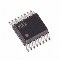
MAX1248BEEE+ Maxim Integrated Products, MAX1248BEEE+ Datasheet - Page 3

MAX1248BEEE+
Manufacturer Part Number
MAX1248BEEE+
Description
IC ADC 10BIT SERIAL 16-QSOP
Manufacturer
Maxim Integrated Products
Datasheet
1.MAX1249BCPE.pdf
(24 pages)
Specifications of MAX1248BEEE+
Number Of Bits
10
Sampling Rate (per Second)
133k
Data Interface
MICROWIRE™, QSPI™, Serial, SPI™
Number Of Converters
1
Power Dissipation (max)
3.6mW
Voltage Supply Source
Single Supply
Operating Temperature
-40°C ~ 85°C
Mounting Type
Surface Mount
Package / Case
16-SSOP (0.150", 3.90mm Width)
Number Of Adc Inputs
4
Architecture
SAR
Conversion Rate
133 KSPs
Resolution
10 bit
Input Type
Voltage
Interface Type
4-Wire (SPI, QSPI, MICROWIRE, TMS320)
Voltage Reference
2.5 V
Supply Voltage (max)
5.25 V
Supply Voltage (min)
2.7 V
Maximum Power Dissipation
842 mW
Maximum Operating Temperature
+ 85 C
Mounting Style
SMD/SMT
Minimum Operating Temperature
- 40 C
Lead Free Status / RoHS Status
Lead free / RoHS Compliant
ELECTRICAL CHARACTERISTICS (continued)
(V
MAX1248—4.7µF capacitor at VREF pin; MAX1249—external reference, VREF = 2.500V applied to VREF pin; T
unless otherwise noted.)
Input Voltage Range, Single-
Ended and Differential (Note 6)
Multiplexer Leakage Current
Input Capacitance
VREF Output Voltage
VREF Short-Circuit Current
VREF Temperature Coefficient
Load Regulation (Note 8)
Capacitive Bypass at VREF
Capacitive Bypass at REFADJ
REFADJ Adjustment Range
VREF Input Voltage Range
(Note 9)
VREF Input Current
VREF Input Resistance
Shutdown VREF Input Current
REFADJ Buffer-Disable Threshold
Capacitive Bypass at VREF
Reference-Buffer Gain
REFADJ Input Current
DIN, SCLK, CS Input High Voltage
DIN, SCLK, CS Input Low Voltage
DIN, SCLK, CS Input Hysteresis
DIN, SCLK, CS Input Leakage
DIN, SCLK, CS Input Capacitance
SHDN Input High Voltage
SHDN Input Mid Voltage
SHDN Input Low Voltage
SHDN Input Current
INTERNAL REFERENCE (MAX1248 only, reference buffer enabled)
EXTERNAL REFERENCE AT VREF (Buffer disabled)
EXTERNAL REFERENCE AT REFADJ
DIGITAL INPUTS (DIN, SCLK, CS, SHDN)
ANALOG/COM INPUTS
DD
= +2.7V to +5.25V; COM = 0V; f
PARAMETER
_______________________________________________________________________________________
+2.7V to +5.25V, Low-Power, 4-Channel,
SYMBOL
V
V
V
HYST
C
V
V
V
I
I
SCLK
IN
SH
SM
SL
IH
S
IL
IN
= 2.0MHz; external clock (50% duty cycle); 15 clocks/conversion cycle (133ksps);
Unipolar, COM = 0V
Bipolar, COM = VREF / 2
On/off leakage current, V
T
MAX1248
0mA to 0.2mA output load
Internal compensation mode
External compensation mode
VREF = 2.500V
Internal compensation mode
External compensation mode
MAX1248
MAX1249
MAX1248
MAX1249
V
V
V
(Note 10)
SHDN = 0V or V
Serial 10-Bit ADCs in QSOP-16
A
DD
DD
IN
= +25°C (Note 7)
= 0V or V
≤ 3.6V
> 3.6V
DD
CONDITIONS
DD
CH_
= 0V or V
DD
V
2.470
V
DD
0.01
MIN
4.7
1.0
0.5
4.7
2.0
3.0
1.1
18
DD -
0
0
- 0.4
±0.01
2.500
±0.01
TYP
0.35
±1.5
0.01
2.06
2.00
±30
100
0.2
16
25
±VREF / 2
0 to VREF
V
A
DD
V
50mV
2.530
= T
MAX
±4.0
DD
±50
±10
150
0.8
- 1.1
0.4
±1
±1
30
10
15
MIN
+
to T
ppm/°C
UNITS
mA
mV
V/V
kΩ
µA
pF
µA
µA
µA
µA
pF
µA
µF
µF
µF
%
V
V
V
V
V
V
V
V
V
V
MAX
3
,


