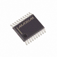
MAX1081BEUP+ Maxim Integrated Products, MAX1081BEUP+ Datasheet - Page 14

MAX1081BEUP+
Manufacturer Part Number
MAX1081BEUP+
Description
IC ADC 10BIT 300KSPS 20-TSSOP
Manufacturer
Maxim Integrated Products
Datasheet
1.MAX1080BEUP.pdf
(24 pages)
Specifications of MAX1081BEUP+
Number Of Bits
10
Sampling Rate (per Second)
300k
Data Interface
MICROWIRE™, QSPI™, Serial, SPI™
Number Of Converters
1
Power Dissipation (max)
8.0mW
Voltage Supply Source
Analog and Digital
Operating Temperature
-40°C ~ 85°C
Mounting Type
Surface Mount
Package / Case
20-TSSOP
Number Of Adc Inputs
8
Architecture
SAR
Conversion Rate
300 KSPs
Resolution
10 bit
Input Type
Differential
Interface Type
4-Wire (SPI, QSPI, MICROWIRE, TMS320)
Voltage Reference
Internal 2.5 V or External
Supply Voltage (max)
3.6 V
Supply Voltage (min)
2.7 V
Maximum Power Dissipation
559 mW
Maximum Operating Temperature
+ 85 C
Mounting Style
SMD/SMT
Minimum Operating Temperature
- 40 C
Lead Free Status / RoHS Status
Lead free / RoHS Compliant
Figure 6 shows the timing for this sequence. Bytes RB2
and RB3 contain the result of the conversion, padded
with three leading zeros, two sub-LSB bits, and one
trailing zero. The total conversion time is a function of
the serial-clock frequency and the amount of idle time
between 8-bit transfers. To avoid excessive T/H droop,
make sure the total conversion time does not exceed
120µs.
In unipolar input mode, the output is straight binary
(Figure 14). For bipolar input mode, the output is two’s
complement (Figure 15). Data is clocked out on the ris-
ing edge of SCLK in MSB-first format.
The external clock not only shifts data in and out but
also drives the analog-to-digital conversion steps.
SSTRB pulses high for one clock period after the last bit
of the control byte. Successive-approximation bit deci-
sions are made and appear at DOUT on each of the
next 12 SCLK rising edges (Figure 6). SSTRB and
DOUT go into a high-impedance state when CS goes
high; after the next CS falling edge, SSTRB outputs a
logic low. Figure 7 shows the detailed serial-interface
timings.
300ksps/400ksps, Single-Supply, Low-Power,
8-Channel, Serial 10-Bit ADCs with Internal Reference
Table 3. Control-Byte Format
14
BIT 7
(MSB)
START
BIT
7(MSB)
6
5
4
3
2
1
0(LSB)
______________________________________________________________________________________
NAME
START
SEL2
SEL1
SEL0
UNI/BIP
SGL/DIF
PD1
PD0
BIT 6
SEL2
DESCRIPTION
The first logic “1” bit after CS goes low defines the beginning of the control byte.
These three bits select which of the eight channels are used for the conversion (Tables 1 and 2).
1 = unipolar, 0 = bipolar. Selects unipolar or bipolar conversion mode. In unipolar mode, an
analog input signal from 0 to V
range from -V
1 = single ended, 0 = pseudo-differential. Selects single-ended or pseudo-differential conver-
sions. In single-ended mode, input signal voltages are referred to COM. In pseudo-differential
mode, the voltage difference between two channels is measured (Tables 1 and 2).
Select operating mode.
PD1
0
0
1
1
BIT 5
SEL1
Serial Clock
PD0
0
1
0
1
Digital Output
REF
/2 to +V
BIT 4
SEL0
Mode
Full power-down
Fast power-down
Reduced power
Normal operation
REF
/2.
REF
The conversion must complete in 120µs or less, or
droop on the sample-and-hold capacitors may degrade
conversion results.
The falling edge of CS does not start a conversion.
The first logic high clocked into DIN is interpreted as a
start bit and defines the first bit of the control byte. A
conversion starts on SCLK’s falling edge, after the eighth
bit of the control byte (the PD0 bit) is clocked into DIN.
The start bit is defined as follows:
Once a start bit has been recognized, the current conver-
sion may only be terminated by pulling SHDN low.
The fastest the MAX1080/MAX1081 can run with CS held
low between conversions is 16 clocks per conversion.
Figure 8 shows the serial-interface timing necessary to
perform a conversion every 16 SCLK cycles. If CS is tied
low and SCLK is continuous, guarantee a start bit by first
clocking in 16 zeros.
can be converted; in bipolar mode, the differential signal can
BIT 3
UNI/BIP
The first high bit clocked into DIN with CS low any
time the converter is idle, e.g., after V
are applied.
The first high bit clocked into DIN after bit 4 of a con-
version in progress is clocked onto the DOUT pin.
BIT 2
SGL/DIF
OR
BIT 1
PD1
Data Framing
DD1
and V
BIT 0
(LSB)
PD0
DD2


