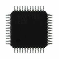
MAX1185ECM+D Maxim Integrated Products, MAX1185ECM+D Datasheet - Page 9

MAX1185ECM+D
Manufacturer Part Number
MAX1185ECM+D
Description
IC ADC 10BIT 20MSPS DUAL 48-TQFP
Manufacturer
Maxim Integrated Products
Datasheet
1.MAX1185ECMD.pdf
(21 pages)
Specifications of MAX1185ECM+D
Number Of Bits
10
Sampling Rate (per Second)
20M
Number Of Converters
2
Power Dissipation (max)
2.43W
Voltage Supply Source
Single Supply
Operating Temperature
-40°C ~ 85°C
Mounting Type
Surface Mount
Package / Case
48-TQFP Exposed Pad, 48-eTQFP, 48-HTQFP, 48-VQFP
Lead Free Status / RoHS Status
Lead free / RoHS Compliant
Internal Reference and Multiplexed Parallel Outputs
2, 6, 11, 14, 15
3, 7, 10, 13, 16
31, 34
32, 33
21–29
PIN
12
17
18
19
20
30
35
36
37
38
39
40
1
4
5
8
9
Dual 10-Bit, 20Msps, 3V, Low-Power ADC with
_______________________________________________________________________________________
SLEEP
OGND
NAME
D0A/B
D1A/B
D2A/B
D3A/B
D4A/B
D5A/B
OV
COM
INA+
INB+
GND
INA-
INB-
CLK
N.C.
V
A/B
T/B
PD
OE
DD
DD
Common-Mode Voltage Input/Output. Bypass to GND with a ≥ 0.1µF capacitor.
Analog Supply Voltage. Bypass each supply pin to GND with a 0.1µF capacitor. Analog
supply accepts a 2.7V to 3.6V input range.
Analog Ground
Channel A Positive Analog Input. For single-ended operation, connect signal source to INA+.
Channel A Negative Analog Input. For single-ended operation, connect INA- to COM.
Channel B Negative Analog Input. For single-ended operation, connect INB- to COM.
Channel B Positive Analog Input. For single-ended operation, connect signal source to INB+.
Converter Clock Input
T/B selects the ADC digital output format.
High: Two’s complement.
Low: Straight offset binary.
Sleep Mode Input.
High: Deactivates the two ADCs, but leaves the reference bias circuit active.
Low: Normal operation.
Power-Down Input.
High: Power-down mode.
Low: Normal operation.
Output Enable Input.
High: Digital outputs disabled.
Low: Digital outputs enabled.
Do not connect.
A/B Data Indicator. This digital output indicates CHA data (A/B = 1) or CHB data (A/B = 0)
to be present on the output. A/B follows the external clock signal with typically 6ns delay.
Output Driver Ground
Output Driver Supply Voltage. Bypass each supply pin to OGND with a 0.1µF capacitor. Output
driver supply accepts a 1.7V to 3.6V input range.
Three-State Digital Output, Bit 0 (LSB). Depending on status of A/B, output data reflects
channel A or channel B data.
Three-State Digital Output, Bit 1. Depending on status of A/B, output data reflects channel A
or channel B data.
Three-State Digital Output, Bit 2. Depending on status of A/B, output data reflects channel A
or channel B data.
Three-State Digital Output, Bit 3. Depending on status of A/B, output data reflects channel A
or channel B data.
Three-State Digital Output, Bit 4. Depending on status of A/B, output data reflects channel A
or channel B data.
Three-State Digital Output, Bit 5. Depending on status of A/B, output data reflects channel A
or channel B data.
FUNCTION
Pin Description
9


