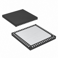
MAX11049ETN+ Maxim Integrated Products, MAX11049ETN+ Datasheet - Page 15

MAX11049ETN+
Manufacturer Part Number
MAX11049ETN+
Description
IC 16BIT PAR 250KSPS 56TQFN-EP
Manufacturer
Maxim Integrated Products
Datasheet
1.MAX11047ETN.pdf
(25 pages)
Specifications of MAX11049ETN+
Number Of Bits
16
Sampling Rate (per Second)
250k
Data Interface
Parallel
Number Of Converters
8
Power Dissipation (max)
2.22W
Voltage Supply Source
Analog and Digital
Operating Temperature
-40°C ~ 85°C
Mounting Type
Surface Mount
Package / Case
56-TQFN Exposed Pad
Conversion Rate
1000 KSPs
Resolution
16 bit
Interface Type
Parallel
Snr
92.3 dB
Voltage Reference
3 V
Supply Voltage (max)
5.25 V
Supply Voltage (min)
2.7 V
Maximum Power Dissipation
3809.5 mW
Maximum Operating Temperature
+ 85 C
Mounting Style
SMD/SMT
Input Voltage
5 V
Minimum Operating Temperature
- 40 C
Lead Free Status / RoHS Status
Lead free / RoHS Compliant
The full-scale analog input voltage is a product of the
reference voltage. For the devices, the input is unipolar
in the range of:
In external reference mode, drive V
4.25V source, resulting in a full-scale input range of
3.662V to 5.188V, respectively.
All analog inputs are fault-protected up to ±20mA. The
devices include an input clamping circuit that activates
when the input voltage at the analog input is above
(V
remains high impedance while the input signal is within
the range of 0V to +V
rent. However, when the input signal exceeds the range
Figure 1. Required Setup for Clamp Circuit
AVDD
+ 300mV) or below -300mV. The clamp circuit
SIGNAL
INPUT
0
______________________________________________________________________________________
to V
Input Range and Protection
SOURCE
+
AVDD
R
REFIO
S
VOLTAGE
PIN
and draws little to no cur-
x
AGNDS
AGND
REFIO
AVDD
CH7
4 096
CH0
5 0
.
†
.
REFIO
**MAX11047/MAX11048/MAX11049
*CONNECTED INTERNALLY ON THE TQFN PARTS
MAX11047/MAX11048/MAX11049/
MAX11057/MAX11058/MAX11059
REFERENCE
BANDGAP
with a 3.0V to
CLAMP
CLAMP
Simultaneous-Sampling ADCs
10kΩ
S/H
S/H
4-/6-/8-Channel, 16-/14-Bit,
EXT REF
INT REF
16-/14-BIT ADC
16-/14-BIT ADC
of 0V to +V
Consequently, to obtain the highest accuracy, ensure
that the input voltage does not exceed the range of 0V
to +V
To make use of the input clamps, connect a resistor
(R
to limit the voltage at the analog input so that the fault
current into the devices does not exceed ±20mA. Note
that the voltage at the analog input pin limits to approxi-
mately 7V during a fault condition so the following
equation can be used to calculate the value of R
where V
source produces during a fault condition.
S
) between the analog input and the voltage source
AVDD
REF
BUF
FAULT_MAX
.
†
AVDD
MAX11049/MAX11059
CONFIGURATION
R
S
REGISTERS
INTERFACE
CONTROL
=
, the clamps begin to turn on.
AND
is the maximum voltage that the
V
FAULT MAX
20
_
mA
WRb
RDb
CSb
CONVST
SHDN
EOCb
DGND
RDC
RDC_SENSE*
DB15**
DB4
DB3/CR3
DB0/CR0
DVDD
−
7
V
S
:
15


