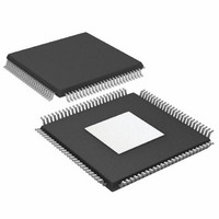
AD9430BSVZ-170 Analog Devices Inc, AD9430BSVZ-170 Datasheet - Page 36

AD9430BSVZ-170
Manufacturer Part Number
AD9430BSVZ-170
Description
IC ADC 12BIT 170MSPS 3.3V100TQFP
Manufacturer
Analog Devices Inc
Datasheet
1.AD9430BSVZ-210.pdf
(44 pages)
Specifications of AD9430BSVZ-170
Data Interface
Parallel
Number Of Bits
12
Sampling Rate (per Second)
170M
Number Of Converters
1
Power Dissipation (max)
1.43mW
Voltage Supply Source
Single Supply
Operating Temperature
-40°C ~ 85°C
Mounting Type
Surface Mount
Package / Case
100-TQFP Exposed Pad
Resolution (bits)
12bit
Sampling Rate
170MSPS
Input Channel Type
Differential, Single Ended
Supply Voltage Range - Digital
3V To 3.6V
Supply Current
335mA
Lead Free Status / RoHS Status
Lead free / RoHS Compliant
Available stocks
Company
Part Number
Manufacturer
Quantity
Price
Company:
Part Number:
AD9430BSVZ-170
Manufacturer:
AD
Quantity:
450
Company:
Part Number:
AD9430BSVZ-170
Manufacturer:
AD
Quantity:
586
Company:
Part Number:
AD9430BSVZ-170
Manufacturer:
Analog Devices Inc
Quantity:
10 000
Part Number:
AD9430BSVZ-170
Manufacturer:
ADI/亚德诺
Quantity:
20 000
Company:
Part Number:
AD9430BSVZ-170-210
Manufacturer:
ADI
Quantity:
120
AD9430
EVALUATION BOARD, LVDS MODE
The AD9430 evaluation board offers an easy way to test the
AD9430 in LVDS mode. (The board is also compatible with the
AD9411.) It requires a clock source, an analog input signal, and
a 3.3 V power supply. The clock source is buffered on the board
to provide the clocks for the ADC, latches, and a data-ready
signal. The digital outputs and output clocks are available at a
40-pin connector, P23. The board has several different modes of
operation and is shipped in the following configurations:
•
•
•
Note that the AD9430 LVDS evaluation board does not
interface directly with the standard Analog Devices dual-
channel data capture board (HSC-ADC-EVAL-DC). An LVDS-
to-CMOS translation board is required and is available from
Analog Devices. (No translation board is required for the
AD9430 CMOS evaluation board.)
POWER CONNECTOR
Power is supplied to the board via a detachable 8-lead power
strip (two 4-pin blocks). In Table 12, VCC, DRVDD, and VDL
are the minimum required power connections, and the
LVEL16 clock buffer can be powered from VCC or VDL at
the E47 jumper.
Table 12. Power Connector, LVDS Mode
VCC 3.3 V
DRVDD 3.3 V
VDL 3.3 V
EXT_VREF
ANALOG INPUTS
The evaluation board accepts a 1.3 V p-p analog input signal
centered at ground at SMB Connector J4. This signal is
terminated to ground through 50 Ω by R16. The input can be
alternatively terminated at the T1 transformer secondary by
R13 and R14. T1 is a wideband RF transformer providing the
single-ended-to-differential conversion, allowing the ADC to
be driven differentially and minimizing even-order harmonics.
An optional second transformer, T2, can be placed following T1
if desired. This provides some performance advantage
(~1 to 2 dB) for high analog input frequencies (>100 MHz). If
T2 is placed, two shorting traces at the pads need to be cut. The
analog signal can be low-pass filtered by R41, C12 and R42, and
C13 at the ADC input. A wideband differential amplifier
(AD8351) can be configured on the PCB for dc-coupled
applications. Remove C6, C15, and C30 to prevent transformer
loading of the amp. See Figure 67, Figure 68, and Figure 69 for
more information.
Offset binary
Internal voltage reference
Full-scale adjust = low
Analog supply for ADC (350 mA)
Output supply for ADC (50 mA)
Supply for support logic
Optional external reference input
Rev. E | Page 36 of 44
GAIN
Full scale is set at E17 to E19, E17 to E18 sets S5 low, full scale =
1.5 V differential; E17 to E19 sets S5 high, full scale = 0.75 V
differential. Best performance is obtained at 1.5 V full scale.
CLOCK
The CLOCK input is terminated to ground through a 50 Ω
resistor at SMB connector J5. The input is ac coupled to a high
speed differential receiver (LVEL16) that provides the required
low jitter, fast edge rates needed for optimum performance.
J5 input should be >0.5 V p-p. Power to the LVEL16 is set at
Jumper E47. E47 to E45 powers the buffer from AVDD; E47 to
E46 powers the buffer from VCLK/V_XTAL (not in Table 11).
VOLTAGE REFERENCE
The AD9430 has an internal 1.23 V voltage reference. The ADC
uses the internal reference as the default when jumpers E24 to
E27 and E25 to E26 are left open. The full scale can be increased
by placing optional resistor R3. The required value varies with
the process and needs to be tuned for the specific application.
Full scale can similarly be reduced by placing R4; tuning is
required here as well. An external reference can be used by
shorting the SENSE pin to 3.3 V (place jumper E26 to E25).
Jumper E27 to E24 connects the ADC VREF pin to the
EXT_VREF pin at the power connector.
DATA FORMAT SELECT
Data format select (DFS) sets the output data format of the ADC.
Setting DFS low (E1 to E2) sets the output format to be offset
binary; setting DFS high (E1 to E3) sets the output to twos
complement.
DATA OUTPUTS
The ADC LVDS digital outputs are routed directly to the
connector at the card edge. Resistor pads have been placed at
the output connector to allow for termination if the connector
receiving logic does not have the required differential
termination for the data bits and DCO. Each output trace pair
should be terminated differentially at the far end of the line
with a single 100 Ω resistor.
CRYSTAL OSCILLATOR
An optional crystal oscillator can be placed on the board to
serve as a clock source for the PCB. Power to the oscillator is
through the VDL pin at the power connector. If an oscillator is
used, ensure proper termination for best results. The board has
been tested with a Valpey Fisher VF561 and a Vectron JN00158-
163.84.


