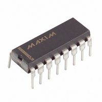
MX7705EPE+ Maxim Integrated Products, MX7705EPE+ Datasheet - Page 24

MX7705EPE+
Manufacturer Part Number
MX7705EPE+
Description
IC ADC 16BIT 2CH 16-DIP
Manufacturer
Maxim Integrated Products
Datasheet
1.MX7705EPE.pdf
(33 pages)
Specifications of MX7705EPE+
Number Of Bits
16
Sampling Rate (per Second)
500
Data Interface
MICROWIRE™, QSPI™, Serial, SPI™
Number Of Converters
1
Voltage Supply Source
Single Supply
Operating Temperature
-40°C ~ 85°C
Mounting Type
Through Hole
Package / Case
16-DIP (0.300", 7.62mm)
Lead Free Status / RoHS Status
Lead free / RoHS Compliant
Set CLK = 0 for optimal performance if the external
clock frequency is 1MHz with CLKDIV = 0 or 2MHz with
CLKDIV = 1.
FS1, FS0: (Default = 0, 1) Filter-Selection Bits. These bits
determine the output data rate and the digital-filter cutoff
frequency. See Table 13 for FS1 and FS0 settings.
Recalibrate when the filter characteristics are changed.
16-Bit, Low-Power, 2-Channel,
Sigma-Delta ADC
Table 10. Operating-Mode Selection
Table 11. PGA Gain Selection
24
MD1
0
0
1
1
G2
______________________________________________________________________________________
0
0
0
0
1
1
1
1
MD0
0
1
0
1
G1
0
0
1
1
0
0
1
1
Normal Mode. Use this mode to perform normal conversions on the selected analog input channel.
Self-Calibration Mode. This mode performs self-calibration on the selected channel determined from CH0 and
CH1 selection bits in the communications register (Table 6). Upon completion of self-calibration, the device
returns to normal mode with MD0, MD1 returning to 0, 0. The DRDY output bit goes high when self-calibration is
requested and returns low when the calibration is complete and a new data word is in the data register. Self-
calibration performs an internal zero-scale and full-scale calibration. The analog inputs of the device are shorted
together internally during zero-scale calibration and connected to an internally generated (V
voltage during full-scale calibration. The offset and gain registers for the selected channel are automatically
updated with the calibration data.
Zero-Scale System-Calibration Mode. This mode performs zero-scale calibration on the selected channel
determined from CH0 and CH1 selection bits in the communications register (Table 6). The DRDY output bit
goes high when calibration is requested and returns low when the calibration is complete and a new data word
is in the data register. Performing zero-scale calibration compensates for any DC offset voltage present in the
ADC and system. Ensure that the analog input voltage is stable within 1/2 LSB for the duration of the calibration
sequence. The offset register for the selected channel is updated with the zero-scale system-calibration data.
Upon completion of calibration, the device returns to normal mode with MD0, MD1 returning to 0, 0.
Full-Scale System-Calibration Mode. This mode performs full-scale system calibration on the selected channel
determined by the CH0 and CH1 selection bits in the communications register. This calibration assigns a full-
scale output code to the voltage present on the selected channel. Ensure that the analog input voltage is stable
within 1/2 LSB for the duration of the calibration sequence. The DRDY output bit goes high during calibration
and returns low when the calibration is complete and a new data word is in the data register. The gain register
for the selected channel is updated with the full-scale system-calibration data. Upon completion of calibration,
the device returns to normal mode with MD0, MD1 returning to 0, 0.
G0
0
1
0
1
0
1
0
1
PGA GAIN
128
16
32
64
1
2
4
8
OPERATING MODE
The data register is a 16-bit register that can be read
and written. Figure 9 shows how to read conversion
results using the data register. A write to the data regis-
ter is not required, but if the data register is written, the
device does not return to its normal state of waiting for
a write to the communications register until all 16 bits
have been written. The 16-bit data word written to the
data register is ignored.
The data from the data register is read through DOUT.
DOUT changes on the falling edge of SCLK and is valid
on the rising edge of SCLK. The data register format is
16-bit straight binary for unipolar mode with zero scale
equal to 0x0000, and offset binary for bipolar mode
with zero scale equal to 0x1000.
REF
/ selected gain)
Data Register


