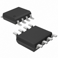
MAX1241CESA+ Maxim Integrated Products, MAX1241CESA+ Datasheet - Page 11

MAX1241CESA+
Manufacturer Part Number
MAX1241CESA+
Description
IC ADC 12BIT SERIAL 8-SOIC
Manufacturer
Maxim Integrated Products
Datasheet
1.MAX1241BCSA.pdf
(15 pages)
Specifications of MAX1241CESA+
Number Of Bits
12
Sampling Rate (per Second)
73k
Data Interface
MICROWIRE™, QSPI™, Serial, SPI™
Number Of Converters
1
Power Dissipation (max)
471mW
Voltage Supply Source
Single Supply
Operating Temperature
-40°C ~ 85°C
Mounting Type
Surface Mount
Package / Case
8-SOIC (0.154", 3.90mm Width)
Lead Free Status / RoHS Status
Lead free / RoHS Compliant
End of conversion (EOC) is signaled by DOUT going
high. DOUT’s rising edge can be used as a framing
signal. SCLK shifts the data out of this register any time
after the conversion is complete. DOUT transitions on
SCLK’s falling edge. The next falling clock edge pro-
duces the MSB of the conversion at DOUT, followed by
the remaining bits. Since there are 12 data bits and one
leading high bit, at least 13 falling clock edges are
needed to shift out these bits. Extra clock pulses occur-
ring after the conversion result has been clocked out,
and prior to a rising edge of CS, produce trailing zeros
at DOUT and have no effect on converter operation.
Minimum cycle time is accomplished by using DOUT’s
rising edge as the EOC signal. Clock out the data with
12.5 clock cycles at full speed. Pull CS high after reading
Figure 9. Detailed Serial-Interface Timing
Figure 10. Unipolar Transfer Function, Full Scale (FS) = V
1 LSB, Zero Scale (ZS) = GND
INTERNAL
11…111
11…110
11…101
00…011
00…010
00…001
00…000
DOUT
SCLK
T/H
CS
OUTPUT CODE
0
(TRACK/ACQUIRE)
1
INPUT VOLTAGE (LSBs)
2
______________________________________________________________________________________
t
APR
3
t
t
DV
CS0
FULL-SCALE
TRANSITION
(HOLD)
t
CONV
FS - 3/2 LSB
FS = V
1 LSB = V
FS
12-Bit Serial ADCs in 8-Pin SO
REF
4096
- 1 LSB
REF
t
STR
REF
…
…
…
…
-
t
DO
the conversion’s LSB. After the specified minimum time
(t
conversion.
The data output from the MAX1240/MAX1241 is binary,
and Figure 10 depicts the nominal transfer function.
Code transitions occur halfway between successive-
integer LSB values. If V
610µV or 2.500V/4096.
The MAX1240/MAX1241 serial interface is fully compat-
ible with SPI/QSPI and MICROWIRE standard serial
interfaces (Figure 11).
If a serial interface is available, set the CPU’s serial
interface in master mode so the CPU generates the ser-
ial clock. Choose a clock frequency up to 2.1MHz.
1) Use a general-purpose I/O line on the CPU to pull CS
2) Wait the for the maximum conversion time specified
3) Activate SCLK for a minimum of 13 clock cycles. The
4) Pull CS high at or after the 13th falling clock edge. If
____________Applications Information
CS
low. Keep SCLK low.
before activating SCLK. Alternatively, look for a DOUT
rising edge to determine the end of conversion.
first falling clock edge produces the MSB of the
DOUT conversion. DOUT output data transitions on
SCLK’s falling edge and is available in MSB-first for-
mat. Observe the SCLK to DOUT valid timing char-
acteristic. Data can be clocked into the µP on
SCLK’s rising edge.
CS remains low, trailing zeros are clocked out after
the LSB.
), CS can be pulled low again to initiate the next
t
CH
B2
(TRACK/ACQUIRE)
Output Coding and Transfer Function
Connection to Standard Interfaces
t
+2.7V, Low-Power,
CL
B1
B0
REF
= +2.500V, then 1 LSB =
t
TR
t
CS
11


