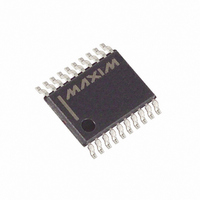
MAX1146BCUP+ Maxim Integrated Products, MAX1146BCUP+ Datasheet - Page 13

MAX1146BCUP+
Manufacturer Part Number
MAX1146BCUP+
Description
IC ADC 14BIT 116KSPS 20-TSSOP
Manufacturer
Maxim Integrated Products
Datasheet
1.MAX1147BEUP.pdf
(25 pages)
Specifications of MAX1146BCUP+
Number Of Bits
14
Sampling Rate (per Second)
116k
Data Interface
MICROWIRE™, QSPI™, Serial, SPI™
Number Of Converters
1
Power Dissipation (max)
879mW
Voltage Supply Source
Single Supply
Operating Temperature
0°C ~ 70°C
Mounting Type
Surface Mount
Package / Case
20-TSSOP
Lead Free Status / RoHS Status
Lead free / RoHS Compliant
The MAX1146–MAX1149 feature input tracking circuitry
with a 3.0MHz small-signal bandwidth. The 3.0MHz
input bandwidth makes it possible to digitize high-
speed transient events and measure periodic signals
with bandwidths exceeding the ADC’s sampling rate by
using undersampling techniques. To avoid high fre-
quency signals being aliased into the frequency band
of interest, anti-alias filtering is recommended.
Internal protection diodes clamp the analog input to
V
to swing from (AGND - 0.3V) to (V
causing damage to the device. For accurate conver-
sions, the inputs must not go more than 50mV below
AGND or above V
Note: If the analog input exceeds 50mV beyond the sup-
ply rails, limit the current to 2mA.
Figure 6. Equivalent Input Circuit
DD
and AGND. These diodes allow the analog inputs
DD
______________________________________________________________________________________
COM
.
CH0
CH1
CH2
CH3
CH4
CH5
CH6
CH7
Analog Input Protection
ANALOG INPUT MUX
Input Bandwidth
DD
+ 0.3V) without
Multichannel, True-Differential,
IN+
IN-
HOLD
HOLD
HOLD
TRACK
C
C
T/H+
T/H-
Use the circuit of Figure 7 to quickly evaluate the
MAX1148/MAX1149. The MAX1148/MAX1149 require a
control byte to be written to DIN using SCLK before
each conversion. Connecting DIN to V
SCLK feeds in a control byte of $FF HEX (see Table 1).
Trigger single-ended unipolar conversions on CH7 in
external clock mode without powering down between
conversions. In external clock mode, the SSTRB output
pulses high for two clock periods before the MSB of the
14-bit conversion result is shifted out of DOUT. Varying
the analog input to CH7 alters the sequence of bits
from DOUT. A total of 18 clock cycles are required per
conversion (Figure 10). All transitions of the SSTRB and
DOUT outputs occur on the falling edge of SCLK.
TRACK
TRACK
Serial, 14-Bit ADCs
REF
REF
14-BIT
CAPACITIVE
DAC
14-BIT
CAPACITIVE
DAC
MAX1148
MAX1149
DD
Quick Look
and clocking
13


