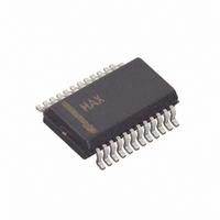
MAX1292AEEG+ Maxim Integrated Products, MAX1292AEEG+ Datasheet

MAX1292AEEG+
Specifications of MAX1292AEEG+
Related parts for MAX1292AEEG+
MAX1292AEEG+ Summary of contents
Page 1
... QSOP MAX1290BEEI -40°C to +85°C 28 QSOP Ordering Information continued at end of data sheet. ________________________________________________________________ Maxim Integrated Products For pricing, delivery, and ordering information, please contact Maxim/Dallas Direct! at 1-888-629-4642, or visit Maxim’s website at www.maxim-ic.com. o 12-Bit Resolution, ±0.5 LSB Linearity o +5V Single-Supply Operation o User-Adjustable Logic Level (+2.7V to +5.5V) o Internal +2 ...
Page 2
ADCs with +2.5V Reference and Parallel Interface ABSOLUTE MAXIMUM RATINGS V to GND ..............................................................-0. GND.........................................................-0.3V to +6V LOGIC CH0–CH7, COM to GND ............................-0. REF, REFADJ to GND.................................-0. ...
Page 3
ADCs with +2.5V Reference and Parallel Interface ELECTRICAL CHARACTERISTICS (continued +5V ±10%, COM = GND, REFADJ = V DD LOGIC cycle unless otherwise noted. Typical values ...
Page 4
ADCs with +2.5V Reference and Parallel Interface ELECTRICAL CHARACTERISTICS (continued +5V ±10%, COM = GND, REFADJ = V DD LOGIC cycle unless otherwise noted. Typical values ...
Page 5
ADCs with +2.5V Reference and Parallel Interface TIMING CHARACTERISTICS (continued +5V ±10%, COM = GND, REFADJ = V DD LOGIC cycle unless otherwise noted. Typical values ...
Page 6
ADCs with +2.5V Reference and Parallel Interface ( +5V +2.500V LOGIC REF INTEGRAL NONLINEARITY vs. DIGITAL OUTPUT CODE 0.5 0.4 0.3 0.2 0.1 0 -0.1 -0.2 -0.3 -0.4 -0.5 ...
Page 7
ADCs with +2.5V Reference and Parallel Interface ( +5V +2.500V LOGIC REF INTERNAL REFERENCE VOLTAGE vs. SUPPLY VOLTAGE 2.53 2.52 2.51 2.50 2.49 2.48 4.50 4.75 5.00 5.25 V ...
Page 8
ADCs with +2.5V Reference and Parallel Interface PIN NAME MAX1290 MAX1292 High Byte Enable. Used to multiplex the 12-bit conversion result HBEN 1: Four MSBs are multiplexed on the data bus. 0: Eight LSBs ...
Page 9
ADCs with +2.5V Reference and Parallel Interface (CH7) (CH6) (CH5) (CH4) ANALOG INPUT CH3 MULTIPLEXER CH2 CH1 CH0 COM CLK CLOCK CS CONTROL LOGIC WR & RD LATCHES INT ( ) ARE FOR MAX1290 ONLY. Figure ...
Page 10
ADCs with +2.5V Reference and Parallel Interface 12-BIT CAPACITIVE DAC REF INPUT C HOLD MUX ZERO – + CH0 CH1 12pF CH2 R IN 800Ω CH3 C SWITCH HOLD CH4 TRACK AT THE SAMPLING INSTANT, CH5 ...
Page 11
ADCs with +2.5V Reference and Parallel Interface conversion. The sampling interval occurs at the end of the acquisition interval. The ACQMOD (acquisition mode) bit in the input control byte (Table 1) offers two options for acquiring ...
Page 12
ADCs with +2.5V Reference and Parallel Interface CSWS CONTROL D7–D0 BYTE ACQMOD = "0" HIGH-Z INT RD HBEN HIGH-Z DOUT Figure 4. Conversion Timing Using Internal Acquisition ...
Page 13
ADCs with +2.5V Reference and Parallel Interface can be used. At power-up, the MAX1290/MAX1292 enter the default external clock mode. Select internal clock mode to release the µP from the burden of running the SAR conversion ...
Page 14
ADCs with +2.5V Reference and Parallel Interface Digital Interface Input (control byte) and output data are multiplexed on a three-state parallel interface. This parallel interface (I/O) can easily be interfaced with standard µPs. The signals CS, ...
Page 15
ADCs with +2.5V Reference and Parallel Interface Table 5. Data-Bus Output ( Parallel Interface) PIN HBEN = 0 HBEN = 1 D0 Bit 0 (LSB) Bit 8 D1 Bit 1 Bit 9 D2 Bit ...
Page 16
ADCs with +2.5V Reference and Parallel Interface only 50µs is required after power-up. Enter standby mode by performing a dummy conversion with the con- trol byte specifying standby mode. Note: Bypass capacitors larger than 4.7µF between ...
Page 17
ADCs with +2.5V Reference and Parallel Interface High-frequency noise in the power supply (V influence the proper operation of the ADC’s fast com- parator. Bypass V to the star ground with a network DD of two ...
Page 18
ADCs with +2.5V Reference and Parallel Interface SUPPLIES 3V/5V V 4.7µ 5Ω 0.1µF V GND DD MAX1036 MAX1037 MAX1038 MAX1039 *OPTIONAL Figure 11. Power-Supply and Grounding Connections Signal-to-Noise Ratio For a waveform perfectly reconstructed ...
Page 19
ADCs with +2.5V Reference and Parallel Interface CLK V LOGIC MAX1290 REF µP WR REFADJ CONTROL INPUTS RD HBEN INT CH7 D7 CH6 CH5 D6 CH4 D5 CH3 D4 CH2 D3/D11 CH1 D2/D10 ...
Page 20
... Maxim cannot assume responsibility for use of any circuitry other than circuitry entirely embodied in a Maxim product. No circuit patent licenses are implied. Maxim reserves the right to change the circuitry and specifications without notice at any time. 20 ____________________Maxim Integrated Products, 120 San Gabriel Drive, Sunnyvale, CA 94086 408-737-7600 © 2002 Maxim Integrated Products Printed USA is a registered trademark of Maxim Integrated Products ...


