MAX19507ETM+ Maxim Integrated Products, MAX19507ETM+ Datasheet - Page 12
MAX19507ETM+
Manufacturer Part Number
MAX19507ETM+
Description
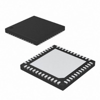
IC ADC 8BIT 2CH 130MSPS 48TQFN
Manufacturer
Maxim Integrated Products
Datasheet
1.MAX19507ETM.pdf
(35 pages)
Specifications of MAX19507ETM+
Number Of Bits
8
Sampling Rate (per Second)
130M
Data Interface
Serial, Parallel
Number Of Converters
2
Power Dissipation (max)
171mW
Voltage Supply Source
Analog and Digital
Operating Temperature
-40°C ~ 85°C
Mounting Type
Surface Mount
Package / Case
48-TQFN Exposed Pad
Lead Free Status / RoHS Status
Lead free / RoHS Compliant


Dual-Channel, 8-Bit, 130Msps ADC
12
1, 12, 13, 48
17, 18
21, 22
25, 36
32, 33
______________________________________________________________________________________
PIN
10
11
14
15
16
19
20
23
24
26
27
28
29
30
31
34
35
37
38
39
2
3
4
5
6
7
8
9
DCLKB
NAME
REFIO
DORB
OVDD
AVDD
SHDN
SPEN
SYNC
CLK+
INA+
INB+
CLK-
CMA
CMB
GND
INA-
INB-
D0B
D1B
D2B
D3B
D4B
D5B
D6B
D7B
D0A
D1A
D2A
D3A
D4A
I.C.
I.C.
I.C.
Analog Supply Voltage. Bypass each AVDD input pair (1, 48) and (12, 13) to GND with 0.1µF.
Channel A Common-Mode Input-Voltage Reference
Channel A Positive Analog Input
Channel A Negative Analog Input
Active-Low SPI Enable. Drive high to enable parallel programming mode.
Reference Input/Output. To use internal reference, bypass to GND with a > 0.1µF capacitor. See
the Reference Input/Output (REFIO) section for external reference adjustment.
Active-High Power-Down. If SPEN is high (parallel programming mode), a register reset is initiated
on the falling edge of SHDN.
Internally Connected. Leave unconnected.
Channel B Positive Analog Input
Channel B Negative Analog Input
Channel B Common-Mode Input-Voltage Reference
Clock-Divider Mode Synchronization Input
Clock Positive Input
Clock Negative Input. If CLK- is connected to ground, CLK+ is a single-ended logic-level clock
input. Otherwise, CLK+/CLK- are self-biased differential clock inputs.
Ground. Connect all ground inputs and EP (exposed pad) together.
Channel B Data Over Range
Channel B Data Clock
Internally Connected. Leave unconnected.
Channel B Three-State Digital Output, Bit 0 (LSB)
Channel B Three-State Digital Output, Bit 1
Digital Supply Voltage. Bypass each OVDD input to GND with a 0.1µF capacitor.
Channel B Three-State Digital Output, Bit 2
Channel B Three-State Digital Output, Bit 3
Channel B Three-State Digital Output, Bit 4
Channel B Three-State Digital Output, Bit 5
Channel B Three-State Digital Output, Bit 6
Channel B Three-State Digital Output, Bit 7 (MSB)
Internally Connected. Leave unconnected.
Channel A Three-State Digital Output, Bit 0 (LSB)
Channel A Three-State Digital Output, Bit 1
Channel A Three-State Digital Output, Bit 2
Channel A Three-State Digital Output, Bit 3
Channel A Three-State Digital Output, Bit 4
FUNCTION
Pin Description
Related parts for MAX19507ETM+
Image
Part Number
Description
Manufacturer
Datasheet
Request
R

Part Number:
Description:
MAX7528KCWPMaxim Integrated Products [CMOS Dual 8-Bit Buffered Multiplying DACs]
Manufacturer:
Maxim Integrated Products
Datasheet:
Part Number:
Description:
Single +5V, fully integrated, 1.25Gbps laser diode driver.
Manufacturer:
Maxim Integrated Products
Datasheet:
Part Number:
Description:
Single +5V, fully integrated, 155Mbps laser diode driver.
Manufacturer:
Maxim Integrated Products
Datasheet:
Part Number:
Description:
VRD11/VRD10, K8 Rev F 2/3/4-Phase PWM Controllers with Integrated Dual MOSFET Drivers
Manufacturer:
Maxim Integrated Products
Datasheet:
Part Number:
Description:
Highly Integrated Level 2 SMBus Battery Chargers
Manufacturer:
Maxim Integrated Products
Datasheet:
Part Number:
Description:
Current Monitor and Accumulator with Integrated Sense Resistor; ; Temperature Range: -40°C to +85°C
Manufacturer:
Maxim Integrated Products
Part Number:
Description:
TSSOP 14/A�/RS-485 Transceivers with Integrated 100O/120O Termination Resis
Manufacturer:
Maxim Integrated Products
Part Number:
Description:
TSSOP 14/A�/RS-485 Transceivers with Integrated 100O/120O Termination Resis
Manufacturer:
Maxim Integrated Products
Part Number:
Description:
QFN 16/A�/AC-DC and DC-DC Peak-Current-Mode Converters with Integrated Step
Manufacturer:
Maxim Integrated Products
Part Number:
Description:
TDFN/A/65V, 1A, 600KHZ, SYNCHRONOUS STEP-DOWN REGULATOR WITH INTEGRATED SWI
Manufacturer:
Maxim Integrated Products
Part Number:
Description:
Integrated Temperature Controller f
Manufacturer:
Maxim Integrated Products
Part Number:
Description:
SOT23-6/I�/45MHz to 650MHz, Integrated IF VCOs with Differential Output
Manufacturer:
Maxim Integrated Products
Part Number:
Description:
SOT23-6/I�/45MHz to 650MHz, Integrated IF VCOs with Differential Output
Manufacturer:
Maxim Integrated Products
Part Number:
Description:
EVALUATION KIT/2.4GHZ TO 2.5GHZ 802.11G/B RF TRANSCEIVER WITH INTEGRATED PA
Manufacturer:
Maxim Integrated Products
Part Number:
Description:
QFN/E/DUAL PCIE/SATA HIGH SPEED SWITCH WITH INTEGRATED BIAS RESISTOR
Manufacturer:
Maxim Integrated Products
Datasheet: