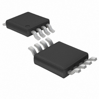
LTC1197CMS8 Linear Technology, LTC1197CMS8 Datasheet - Page 12

LTC1197CMS8
Manufacturer Part Number
LTC1197CMS8
Description
IC ADC 10BIT 500KHZ SHTDWN 8MSOP
Manufacturer
Linear Technology
Datasheet
1.LTC1197CS8PBF.pdf
(28 pages)
Specifications of LTC1197CMS8
Number Of Bits
10
Sampling Rate (per Second)
500k
Data Interface
MICROWIRE™, Serial, SPI™
Number Of Converters
1
Power Dissipation (max)
25mW
Voltage Supply Source
Single Supply
Operating Temperature
0°C ~ 70°C
Mounting Type
Surface Mount
Package / Case
8-TSSOP, 8-MSOP (0.118", 3.00mm Width)
Lead Free Status / RoHS Status
Contains lead / RoHS non-compliant
Available stocks
Company
Part Number
Manufacturer
Quantity
Price
Company:
Part Number:
LTC1197CMS8
Manufacturer:
LT
Quantity:
10 000
Part Number:
LTC1197CMS8#PBF
Manufacturer:
LINEAR/凌特
Quantity:
20 000
LTC1197/LTC1197L
LTC1199/LTC1199L
APPLICATIO S I FOR ATIO
OVERVIEW
The LTC1197/LTC1197L/LTC1199/LTC1199L are 10-bit
switched-capacitor A/D converters. These sampling ADCs
typically draw 5mA of supply current when sampling up to
500kHz (800 A at 2.7V sampling up to 250kHz). Supply
current drops linearly as the sample rate is reduced (see
Supply Current vs Sample Rate in the Typical Perfor-
mance Characteristics). The ADCs automatically power
down when not performing a conversion, drawing only
leakage current. They are packaged in 8-pin MSOP and SO
packages. The LTC1197L/LTC1199L operate on a single
supply ranging from 2.7V to 4V. The LTC1197 operates on
a single supply ranging from 4V to 9V while the LTC1199
operates from 4V to 6V.
These ADCs contain a 10-bit, switched-capacitor ADC, a
sample-and-hold and a serial port (see Block Diagram).
Although they share the same basic design, the LTC1197/
LTC1197L and LTC1199/LTC1199L differ in some re-
spects. The LTC1197/LTC1197L have a differential input
and have an external reference input pin. They can mea-
sure signals floating on a DC common mode voltage and
can operate with reduced spans down to 200mV. Reduc-
ing the span allows it to achieve 200 V resolution. The
LTC1199/LTC1199L have a 2-channel input multiplexer
with the reference connected to the supply (V
can convert the input voltage of either channel with re-
spect to ground or the difference between the voltages of
the two channels.
12
D
OUT
CLK
CS
*AFTER COMPLETING THE DATA TRANSFER, IF FURTHER CLOCKS ARE APPLIED WITH CS LOW,
THE ADC WILL OUTPUT ZEROS INDEFINITELY
U
1
(1.5 CLKs)
HI-Z
t
SMPL
t
suCS
U
2
NULL
BITS
3
W
4
Figure 1. LTC1197/LTC1197L Operating Sequence
B9
5
CC
B8
U
) pin. They
6
B7
t
CYC
7
(14 CLKs )*
(10.5 CLKs)
B6
t
CONV
8
B5
SERIAL INTERFACE
The LTC1199/LTC1199L communicate with microproces-
sors and other external circuitry via a synchronous, half
duplex, 4-wire serial interface while the LTC1197/
LTC1197L use a 3-wire interface (see Operating Sequence
in Figures 1 and 2). These interfaces are compatible with
both SPI and MICROWIRE protocols without requiring any
additional glue logic (see MICROPROCESSOR INTER-
FACES: Motorola SPI).
DATA TRANSFER
The CLK synchronizes the data transfer with each bit being
transmitted and captured on the rising CLK edge in both
transmitting and receiving systems. The LTC1199/
LTC1199L first receives input data and then transmits
back the A/D conversion result (half duplex). Because of
the half-duplex operation, D
together allowing transmission over just three wires: CS,
CLK and DATA (D
Data transfer is initiated by a falling chip select (CS) signal.
After CS falls the LTC1199/LTC1199L look for a start bit on
the D
word is shifted into the D
LTC1199/LTC1199L and starts the conversion. After two
null bits, the result of the conversion is output on the D
line in MSB-first format. At the end of the data exchange
CS should be brought high. This resets the LTC1199/
LTC1199L in preparation for the next data exchange.
Bringing CS high after the conversion also minimizes
supply current if CLK is left running.
9
B4
IN
input. After the start bit is received, the 3-bit input
10
B3
t
dDO
11
B2
IN
12
/D
B1
OUT
13
).
B0*
POWER
IN
DOWN
14
input which configures the
IN
and D
Hi-Z
1
1197/99 F01
OUT
may be tied
OUT


