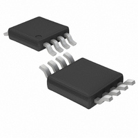
LTC1197IMS8#TRPBF Linear Technology, LTC1197IMS8#TRPBF Datasheet - Page 17

LTC1197IMS8#TRPBF
Manufacturer Part Number
LTC1197IMS8#TRPBF
Description
IC ADC 10BIT 500KHZ SHTDWN 8MSOP
Manufacturer
Linear Technology
Datasheet
1.LTC1197CS8PBF.pdf
(28 pages)
Specifications of LTC1197IMS8#TRPBF
Number Of Bits
10
Sampling Rate (per Second)
500k
Data Interface
MICROWIRE™, Serial, SPI™
Number Of Converters
1
Power Dissipation (max)
25mW
Voltage Supply Source
Single Supply
Operating Temperature
-40°C ~ 85°C
Mounting Type
Surface Mount
Package / Case
8-TSSOP, 8-MSOP (0.118", 3.00mm Width)
Lead Free Status / RoHS Status
Lead free / RoHS Compliant
Available stocks
Company
Part Number
Manufacturer
Quantity
Price
APPLICATIO S I FOR ATIO
ANALOG INPUTS
Because of the capacitive redistribution A/D conversion
techniques used, the analog inputs of the LTC1197/
LTC1197L/LTC1199/LTC1199L have capacitive switching
input current spikes. These current spikes settle quickly
and do not cause a problem if source resistances are less
than 200
LT
source resistances are used or if slow settling op amps
drive the inputs, take care to ensure that the transients
caused by the current spikes settle completely before the
conversion begins.
“+” Input Settling
The input capacitor of the LTC1197/LTC1197L is switched
onto the “+” input in the falling edge of CS and the sample
time continues until the second falling CLK edge (see
Figure 1). However, the input capacitor of the LTC1199/
LTC1199L is switched onto “+” input after ODD/SGN is
clocked into the ADC and remains there until the fourth
falling CLK edge (see Figure 5). The sample time is 1.5 CLK
cycles before conversion starts. The voltage on the “+”
®
1224, LT1191, LT1226 or LT1215). However, if large
“+” INPUT
“–” INPUT
or high speed op amps are used (e.g., the
D
CLK
OUT
D
CS
IN
U
U
Figure 5. LTC1199/LTC1199L “+” and “–” Input Settling Windows
W
START
U
SGL/DIFF
input must settle completely within t
perform an accurate conversion. Minimizing R
and C1 will improve the input settling time (see Figure 6).
If a large “+” input source resistance must be used, the
sample time can be increased by using a slower CLK
frequency.
“–” Input Settling
At the end of t
“–” input and conversion starts (see Figures 1 and 5).
During the conversion the “+” input voltage is effectively
“held” by the sample-and-hold and will not affect the
1ST BIT TEST “–” INPUT MUST
ODD/SGN
SAMPLE
SETTLE DURING THIS TIME
V
V
IN
IN
+
–
“+” INPUT MUST
SETTLE DURING
THIS TIME
R
R
SOURCE
SOURCE
t
SMPL
Figure 6. Analog Equivalent Circuit
DUMMY
SMPL
+
–
HOLD
, the input capacitor switches to the
C1
INPUT
C2
INPUT
“–”
“+”
LTC1197/LTC1197L
LTC1199/LTC1199L
t
CONV
DON‘T CARE
R
ON
SMPL
= 200
1197/99 F05
LTC1197/LTC1197L
LTC1199/LTC1199L
for the ADC to
C
IN
= 20pF
1197/99 F06
SOURCE
17
+


