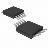
LTC2431IMS#PBF Linear Technology, LTC2431IMS#PBF Datasheet - Page 29

LTC2431IMS#PBF
Manufacturer Part Number
LTC2431IMS#PBF
Description
IC ADC 20BIT DIFFINPUT/REF10MSOP
Manufacturer
Linear Technology
Datasheet
1.LTC2431CMSPBF.pdf
(40 pages)
Specifications of LTC2431IMS#PBF
Number Of Bits
20
Sampling Rate (per Second)
7.5
Data Interface
MICROWIRE™, Serial, SPI™
Number Of Converters
2
Power Dissipation (max)
1mW
Voltage Supply Source
Single Supply
Operating Temperature
-40°C ~ 85°C
Mounting Type
Surface Mount
Package / Case
10-TFSOP, 10-MSOP (0.118", 3.00mm Width)
Lead Free Status / RoHS Status
Lead free / RoHS Compliant
Available stocks
Company
Part Number
Manufacturer
Quantity
Price
APPLICATIO S I FOR ATIO
an infinite bandwidth source and 216nV/ Hz for a single
0.5MHz pole source. From these numbers, it is clear that
particular attention must be given to the design of external
amplification circuits. Such circuits face the
simultaneous requirements of very low bandwidth (just a
few Hz) in order to reduce the output referred noise and
relatively high bandwidth (at least 500kHz) necessary to
drive the input switched-capacitor network. A possible
solution is a high gain, low bandwidth amplifier stage
followed by a high bandwidth unity-gain buffer.
When external amplifiers are driving the LTC2430/
LTC2431, the ADC input referred system noise calculation
can be simplified by Figure 29. The noise of an amplifier
driving the LTC2430/LTC2431 input pin can be modeled
as a band-limited white noise source. Its bandwidth can be
Figure 28. Input Signal Bandwidth Using the Internal Oscillator
Figure 26. Resolution (Noise
vs Output Data Rate and V
–2
–4
–5
–6
–1
–3
0
22
19
17
15
21
20
18
16
0
DIFFERENTIAL INPUT SIGNAL FREQUENCY (Hz)
0
V
V
F
REF
T
RES = LOG
O
INCM
IN
A
10
= EXT OSC
= 25 C
OUTPUT DATA RATE (READINGS/SEC)
= 0V
–
= GND
1
U
= V
20 30
REFCM
2
(V
F
O
REF
= HIGH
2
U
40
/NOISE
V
V
V
REF
CC
CC
50
= V
= 2.7V
= 2.5V
RMS
3
60
REF
CC
)
= 5V
70
W
RMS
F
O
4
= LOW
80
2431 F28
90 100
2430 F26
1LSB)
5
U
approximated by the bandwidth of a single pole lowpass
filter with a corner frequency f
tral density is n
selector, we can find on the y-axis the noise equivalent
bandwidth freq
width includes the band limiting effects of the ADC internal
calibration and filtering. The noise of the driving amplifier
referred to the converter input and including all these
effects can be calculated as N = n
noise (referred to the LTC2430/LTC2431 input) can now
be obtained by summing as square root of sum of squares
the three ADC input referred noise sources: the LTC2430/
LTC2431 internal noise (2.8 V), the noise of the IN
driving amplifier and the noise of the IN
Figure 29. Input Referred Noise Equivalent Bandwidth
of an Input Connected White Noise Source
1000
Figure 27. Resolution (INL
vs Output Data Rate and V
100
0.1
22
19
17
15
21
20
18
16
10
1
0.1
0
V
V
F
REF
T
RES = LOG
O
INCM
IN
A
i
10
= EXT OSC
= 25 C
i
OUTPUT DATA RATE (READINGS/SEC)
of the input driving amplifier. This band-
= 0V
–
INPUT NOISE SOURCE SINGLE POLE
. From Figure 29, using f
1
= GND
= V
EQUIVALENT BANDWIDTH (Hz)
20 30
LTC2430/LTC2431
REFCM
2
10
(V
V
REF
CC
40
/INL
100
= V
F
F
O
V
O
50
V
REF
MAX
REF
= HIGH
CC
= LOW
1k
i
= 5V
)
. The amplifier noise spec-
= 2.7V
60
= 2.5V
i
• freq
CC
70
MAX
10k 100k 1M
80
–
1LSB)
2431 G29
90 100
i
2430 F27
. The total system
driving amplifier.
i
as the x-axis
29
24301f
+


