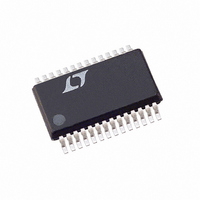
LTC2439-1CGN Linear Technology, LTC2439-1CGN Datasheet - Page 13

LTC2439-1CGN
Manufacturer Part Number
LTC2439-1CGN
Description
IC ADC 16BIT 16CH MCRPWR 28SSOP
Manufacturer
Linear Technology
Datasheet
1.LTC2439-1CGN.pdf
(28 pages)
Specifications of LTC2439-1CGN
Number Of Bits
16
Sampling Rate (per Second)
6.8
Data Interface
MICROWIRE™, Serial, SPI™
Number Of Converters
1
Power Dissipation (max)
1mW
Voltage Supply Source
Single Supply
Operating Temperature
0°C ~ 70°C
Mounting Type
Surface Mount
Package / Case
28-SSOP (0.150", 3.95mm Width)
Lead Free Status / RoHS Status
Contains lead / RoHS non-compliant
Available stocks
Company
Part Number
Manufacturer
Quantity
Price
Part Number:
LTC2439-1CGN
Manufacturer:
LT/凌特
Quantity:
20 000
Part Number:
LTC2439-1CGN#TRPBF
Manufacturer:
LINEAR/凌特
Quantity:
20 000
APPLICATIO S I FOR ATIO
Table 4. LTC2439-1 State Duration
State
CONVERT
SLEEP
DATA OUTPUT
SERIAL INTERFACE PINS
The LTC2439-1 transmits the conversion results and re-
ceives the start of conversion command through a syn-
chronous 4-wire interface. During the conversion and sleep
states, this interface can be used to assess the converter
status and during the data I/O state it is used to read the
conversion result and write in channel selection bits.
Serial Clock Input/Output (SCK)
The serial clock signal present on SCK (Pin 18) is used to
synchronize the data transfer. Each bit of data is shifted out
the SDO pin on the falling edge of the serial clock and each
input bit is shifted in the SDI pin on the rising edge of the
serial clock.
Table 3. LTC2439-1 Output Data Format
Differential Input Voltage
V
V
0.5 • V
0.25 • V
0.25 • V
0
–1LSB
– 0.25 • V
– 0.25 • V
– 0.5 • V
V
*The differential input voltage V
IN
IN
IN
* ≥ 0.5 • V
* < –0.5 • V
*
REF
REF
REF
REF
REF
REF
** – 1LSB
**
** – 1LSB
Operating Mode
Internal Oscillator
External Oscillator
Internal Serial Clock
External Serial Clock with
Frequency f
**
**
** – 1LSB
REF
U
REF
**
**
U
SCK
kHz
IN
= IN
W
Bit 18
EOC
0
0
0
0
0
0
0
0
0
0
+
– IN
–
F
Simultaneous 50Hz/60Hz Rejection
F
with Frequency f
(f
F
(Internal Oscillator)
F
Frequency f
.
O
O
O
O
EOSC
Bit 17
= LOW
= External Oscillator
= LOW
= External Oscillator with
DMY
0
0
0
0
0
0
0
0
0
0
U
/2560 Rejection)
**The differential reference voltage V
EOSC
Bit 16
SIG
1
1
1
1
1
0
0
0
0
0
EOSC
kHz
kHz
Bit 15
MSB
In the Internal SCK mode of operation, the SCK pin is an
output and the LTC2439-1 creates its own serial clock by
dividing the internal conversion clock by 8. In the External
SCK mode of operation, the SCK pin is used as input. The
Internal or External SCK mode is selected on power-up and
then reselected every time a HIGH-to-LOW transition is de-
tected at the CS pin. If SCK is HIGH or floating at power-
up or during this transition, the converter enters the internal
SCK mode. If SCK is LOW at power-up or during this tran-
sition, the converter enters the external SCK mode.
Serial Data Input (SDI)
The serial data input pin, SDI (Pin 20), is used to shift in the
channel control bits during the data output state to prepare
the channel selection for the following conversion.
1
0
0
0
0
1
1
1
1
0
Bit 14
0
1
1
0
0
1
1
0
0
1
Duration
147ms, Output Data Rate ≤ 6.8 Readings/s
20510/f
As Long As CS = HIGH Until CS = LOW and SCK
As Long As CS = LOW But Not Longer Than 1.09ms
(19 SCK cycles)
As Long As CS = LOW But Not Longer Than 152/f
(19 SCK cycles)
As Long As CS = LOW But Not Longer Than 19/f
(19 SCK cycles)
REF
Bit 13
EOSC
0
1
0
1
0
1
0
1
0
1
= REF
s, Output Data Rate ≤ f
+
– REF
Bit 12
0
1
0
1
0
1
0
1
0
1
–
.
…
…
…
…
…
…
…
…
…
…
…
LTC2439-1
EOSC
/20510 Readings/s
Bit 0
0
1
0
1
0
1
0
1
0
1
SCK
EOSC
13
ms
ms
24391fa


