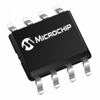
MCP3553-E/MS Microchip Technology, MCP3553-E/MS Datasheet - Page 5

MCP3553-E/MS
Manufacturer Part Number
MCP3553-E/MS
Description
IC ADC 22BIT 2.7V 1CH SPI 8MSOP
Manufacturer
Microchip Technology
Specifications of MCP3553-E/MS
Package / Case
8-TSSOP, 8-MSOP (0.118", 3.00mm Width)
Number Of Bits
22
Sampling Rate (per Second)
60
Data Interface
Serial, SPI™
Number Of Converters
1
Voltage Supply Source
Single Supply
Operating Temperature
-40°C ~ 125°C
Mounting Type
Surface Mount
Architecture
Delta-Sigma
Conversion Rate
0.06 KSPs
Input Type
Voltage
Maximum Operating Temperature
+ 85 C
Mounting Style
SMD/SMT
Minimum Operating Temperature
- 40 C
Lead Free Status / RoHS Status
Lead free / RoHS Compliant
For Use With
MCP355XDV-MS1 - BOARD DEV SENSOR APP MCP355XMCP355XDM-TAS - BOARD DEMO TINY APP SNSR MCP355X
Lead Free Status / Rohs Status
Lead free / RoHS Compliant
DC CHARACTERISTICS (CONTINUED)
TEMPERATURE CHARACTERISTICS
SERIAL TIMINGS
© 2009 Microchip Technology Inc.
Electrical Specifications: Unless otherwise indicated, all parameters apply at -40°C ≤ T
V
applies to entire MCP3550/1/3 family.
Voltage Output Low (SDO/RDY)
Input leakage Current
(CS, SCK)
Internal Pin Capacitance
(CS, SCK, SDO/RDY)
Note 1:
Electrical Specifications: Unless otherwise indicated
Temperature Ranges
Specified Temperature Range
Operating Temperature Range
Thermal Package Resistances
Thermal Resistance, 8L-MSOP
Thermal Resistance, 8L-SOIC
Electrical Specifications: Unless otherwise indicated, all parameters apply at -40°C ≤ T
V
CLK Frequency
CLK High
CLK Low
CLK fall to output data valid
CS low to indicate RDY state
CS minimum low time
RDY flag setup time
CS rise to output disable
CS disable time
Power-up to CS LOW
CS High to Shutdown Mode
REF
DD
= 3.3V or 5.0V, SDO load = 50 pF.
= 2.5V. V
2:
3:
4:
5:
6:
Parameters
Parameters
Parameters
This parameter is established by characterization and not 100% tested.
INL is the difference between the endpoints line and the measured code at the center of the quantization band.
This current is due to the leakage current and the current due to the offset voltage between V
Input impedance is inversely proportional to clock frequency; typical values are for the MCP3550/1 device. V
Characterized by design, but not tested.
Rejection performance depends on internal oscillator accuracy; see Section 4.0 “Device Overview” for more informa-
tion on oscillator and digital filter design. MCP3550/1 device rejection specifications characterized from 49 to 61 Hz.
IN
+ = V
IN
- = V
CM
= V
REF
t
t
CSHSD
PUCSL
Sym
Sym
/2. All ppm units use 2*V
f
t
t
t
t
θ
θ
SCK
t
RDY
t
CSD
t
CSL
Sym
T
T
C
t
DIS
V
DO
SU
LO
HI
JA
JA
I
A
A
INT
OL
LI
Min
Min
-40
-40
90
90
50
20
20
90
—
—
—
—
—
0
0
Min
—
-1
—
149.5
Typ
211
Typ
10
10
—
—
—
—
—
—
—
—
—
—
—
Typ
REF
—
—
5
as full scale range. Unless otherwise noted, specification
+125
Max
Max
+85
90
50
—
—
—
—
—
—
—
—
—
—
5
Max
0.4
—
1
Units
Units
°C/W
°C/W
MHz
°C
°C
ns
ns
ns
ns
ns
ns
ns
ns
µs
µs
Units
µA
pF
V
A
≤ +85°C, V
MCP3550/1/3
V
Note 1
OH
A
= -1 mA, V
DD
≤ +85°C,
Conditions
Conditions
= 2.7V or 5.0V.
IN
+ and V
Conditions
DD
DS21950E-page 5
= 5.0V
IN
-.
REF
= 5V.


