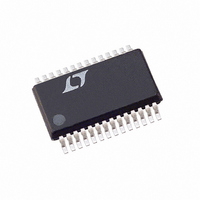
LTC2424CG Linear Technology, LTC2424CG Datasheet - Page 26

LTC2424CG
Manufacturer Part Number
LTC2424CG
Description
IC ADC 20BIT 4CH MICROPWR 28SSOP
Manufacturer
Linear Technology
Datasheet
1.LTC2424CGPBF.pdf
(36 pages)
Specifications of LTC2424CG
Number Of Bits
20
Sampling Rate (per Second)
7.5
Data Interface
MICROWIRE™, Serial, SPI™
Number Of Converters
1
Power Dissipation (max)
1mW
Voltage Supply Source
Single Supply
Operating Temperature
0°C ~ 70°C
Mounting Type
Surface Mount
Package / Case
28-SSOP (0.200", 5.30mm Width)
Lead Free Status / RoHS Status
Contains lead / RoHS non-compliant
Available stocks
Company
Part Number
Manufacturer
Quantity
Price
Part Number:
LTC2424CG#PBF
Manufacturer:
LINEAR/凌特
Quantity:
20 000
Part Number:
LTC2424CG#TRPBF
Manufacturer:
LINEAR/凌特
Quantity:
20 000
APPLICATIONS
LTC2424/LTC2428
Input Current (V
If complete settling occurs on the input, conversion re-
sults will be unaffected by the dynamic input current. If the
settling is incomplete, it does not degrade the linearity
performance of the device. It simply results in an offset/
full-scale shift, see Figure 19. To simplify the analysis of
input dynamic current, two separate cases are assumed:
large capacitance at V
tance at V
If the total capacitance at V
(< 0.01 F), relatively large external source resistances (up
to 20k for 20pF parasitic capacitance) can be tolerated
without any offset/full-scale error. Figures 21 and 22 show
a family of offset and full-scale error curves for various
small valued input capacitors (C
of input source resistance.
For large input capacitor values (C
spikes are averaged by the capacitor into a DC current. The
gain shift becomes a linear function of input source
resistance independent of input capacitance, see Figures
23 and 24. The equivalent input impedance is 16.6M .
26
TUE
0
SOURCE
SIGNAL
INTPUT
IN
V
REF
Figure 20. An RC Network at CH0 to CH7
(C
= FS
Figure 19. Offset/Full-Scale Shift
IN
SET
IN
< 0.01 F).
R
)
–ZS
SOURCE
U
SET
IN
(C
INFORMATION
U
V
IN
REF
V
C
IN
IN
> 0.01 F) and small capaci-
IN
/2
(see Figure 20) is small
IN
< 0.01 F) as a function
IN
C
W
PAR
20pF
> 0.01 F), the input
CH0 TO
CH7
LTC2424/
LTC2428
24248 F20
U
24248 F19
V
REF
This results in 150nA of input dynamic current at the
extreme values of V
V
and full-scale readings for every 10
resistance.
While large capacitance applied to one of the multiplexer
channel inputs may result in offset/full-scale shifts, large
capacitance applied to the MUXOUT/ADCIN results in
linearity errors. The 75 on-resistance of the multiplexer
switch is nonlinear with input voltage. If the capacitance
at node MUXOUT/ADCIN is less than 0.01 F, the linearity
is not degraded. On the other hand, excessive capaci-
tance (>0.01 F) results in incomplete settling as a func-
tion of the multiplexer on-resistance. Hence, the
REF
= 5V). This corresponds to a 0.3ppm shift in offset
Figure 22. Full-Scale Error vs R
–10
–20
–30
–40
–50
10
50
40
20
10
30
Figure 21. Offset vs R
0
0
1
1
V
V
V
T
V
V
V
T
A
CC
REF
IN
A
CC
REF
IN
= 25 C
= 25 C
= 5V
= 0V
= 5V
= 5V
= 5V
= 5V
10
10
C
IN
C
C
IN
C
IN
IN
C
C
= 1000pF
IN
IN
C
= 1000pF
IN
= 100pF
(V
C
IN
= 100pF
100
= 0.01 F
R
100
R
= 0pF
IN
SOURCE
IN
= 0pF
SOURCE
= 0.01 F
= 0V and V
( )
SOURCE
1k
( )
1k
SOURCE
10k
10k
(Small C)
24248 F22
24248 F21
IN
of input source
(Small C)
100k
100k
= V
REF
, when


