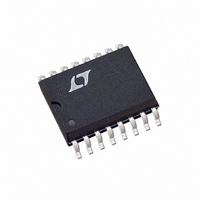
LTC1594CS Linear Technology, LTC1594CS Datasheet - Page 10

LTC1594CS
Manufacturer Part Number
LTC1594CS
Description
IC A/D CONV 12BIT SRL 4CH 16SOIC
Manufacturer
Linear Technology
Datasheet
1.LTC1594CSPBF.pdf
(24 pages)
Specifications of LTC1594CS
Number Of Bits
12
Sampling Rate (per Second)
16.8M
Data Interface
MICROWIRE™, QSPI™, Serial, SPI™
Number Of Converters
1
Power Dissipation (max)
1.6mW
Voltage Supply Source
Single Supply
Operating Temperature
0°C ~ 70°C
Mounting Type
Surface Mount
Package / Case
16-SOIC (0.154", 3.90mm Width)
Lead Free Status / RoHS Status
Contains lead / RoHS non-compliant
Available stocks
Company
Part Number
Manufacturer
Quantity
Price
Company:
Part Number:
LTC1594CS
Manufacturer:
LT
Quantity:
5 510
Part Number:
LTC1594CS
Manufacturer:
LT/凌特
Quantity:
20 000
Company:
Part Number:
LTC1594CS#PBF
Manufacturer:
LT
Quantity:
1 483
Part Number:
LTC1594CS#PBF
Manufacturer:
LINEAR/凌特
Quantity:
20 000
LTC1594/LTC1598
APPLICATIONS
OVERVIEW
The LTC1594/LTC1598 are micropower, 12-bit sampling
A/D converters that feature a 4- and 8-channel multi-
plexer respectively. They typically draw only 320μA of
supply current when sampling at 16.8kHz. Supply cur-
rent drops linearly as the sample rate is reduced (see
Supply Current vs Sample Rate). The ADCs automatically
power down when not performing conversions, drawing
only leakage current. The LTC1594 is available in a 16-pin
narrow SO package and the LTC1598 is packaged in a
24-pin SSOP. Both devices operate on a single supply
from 4.5V to 5.5V.
The LTC1594/LTC1598 contain a 12-bit, switched-
capacitor ADC, sample-and-hold, serial port and an
external reference input pin. In addition, the LTC1594 has
a 4-channel multiplexer and the LTC1598 provides an
8-channel multiplexer (see Block Diagram). They can
measure signals floating on a DC common mode voltage
10
CSMUX = CSADC = CS
COM = GND
MUXOUT
ADCIN =
CH0 TO
D
CH7
CLK
OUT
D
U
IN
INFORMATION
U
EN
Figure 1. LTC1594/LTC1598 Operating Sequence Example: CH2, GND
D2
Hi-Z
D1
W
D0
*AFTER COMPLETING THE DATA TRANSFER, IF FURTHER CLOCKS ARE APPLIED WITH CS LOW,
THE ADC WILL OUTPUT LSB-FIRST DATA THEN FOLLOWED WITH ZEROS INDEFINITELY
t
SMPL
t
ON
t
suCS
U
NULL
BIT
B11
B10
B9
t
CYC
and can operate with reduced spans to 1.5V. Reducing
the spans allow them to achieve 366μV resolution.
The LTC1594/LTC1598 provide separate MUX output
and ADC input pins to form an ideal MUXOUT/ADCIN
loop which economizes signal conditioning. The MUX
and ADC of the devices can also be controlled individually
through separate chip selects to enhance flexibility.
SERIAL INTERFACE
For this discussion we will assume that CSMUX and
CSADC are tied together and will refer to them as simply
CS, unless otherwise specified.
The LTC1594/LTC1598 communicate with the micropro-
cessor and other external circuitry via a synchronous,
half duplex, 4-wire interface (see Operating Sequences in
Figures 1 and 2).
DON’T CARE
B8
B7
t
CONV
B6
B5
B4
B3 B2
B1 B0*
Hi-Z
1594/98 F01
15948fb


