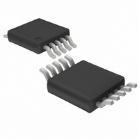
LTC2402CMS#TR Linear Technology, LTC2402CMS#TR Datasheet - Page 13

LTC2402CMS#TR
Manufacturer Part Number
LTC2402CMS#TR
Description
IC ADC 24BIT 2CH MICROPWR 10MSOP
Manufacturer
Linear Technology
Datasheet
1.LTC2401CMSPBF.pdf
(32 pages)
Specifications of LTC2402CMS#TR
Number Of Bits
24
Sampling Rate (per Second)
7.5
Data Interface
MICROWIRE™, Serial, SPI™
Number Of Converters
2
Power Dissipation (max)
1mW
Voltage Supply Source
Single Supply
Operating Temperature
0°C ~ 70°C
Mounting Type
Surface Mount
Package / Case
10-TFSOP, 10-MSOP (0.118", 3.00mm Width)
Lead Free Status / RoHS Status
Contains lead / RoHS non-compliant
Available stocks
Company
Part Number
Manufacturer
Quantity
Price
APPLICATIO S I FOR ATIO
Table 2. LTC2401/LTC2402 Output Data Format
Input Voltage
V
9/8 • V
V
V
3/4V
3/4V
1/2V
1/2V
1/4V
1/4V
0
–1LSB
–1/8 • V
V
*The sub LSBs are valid conversion results beyond the 24-bit level that may be included in averaging or discarded without loss of resolution.
**The sign bit changes state during the 0 code.
disturb the converter operation. If the selection is made
during the conversion state, the result of the conversion in
progress may be outside specifications but the following
conversions will not be affected.
When a fundamental rejection frequency different from
50Hz or 60Hz is required or when the converter must be
synchronized with an outside source, the LTC2401/
LTC2402 can operate with an external conversion clock.
The converter automatically detects the presence of an
external clock signal at the F
oscillator. The frequency f
be at least 2560Hz (1Hz notch frequency) to be detected.
The external clock signal duty cycle is not significant as
long as the minimum and maximum specifications for the
high and low periods t
While operating with an external conversion clock of a
frequency f
than 110dB normal mode rejection in a frequency range
f
rejection as a function of the input frequency deviation
from f
EOSC
+
IN
REF
REF
IN
/0
> 9/8 • V
< –1/8 • V
–
REF
REF
REF
REF
REF
REF
+ 1LSB
REF
/2560 4% and its harmonics. The normal mode
REF
EOSC
+ 1LSB
+ 1LSB
+ 1LSB
REF
REF
/2560 is shown in Figure 4.
EOSC
, the LTC2401/LTC2402 provide better
Bit 31
EOC
0
0
0
0
0
0
0
0
0
0
0
0
0
0
U
HEO
CH SELECT
CH0/CH1
CH0/CH1
CH0/CH1
CH0/CH1
CH0/CH1
CH0/CH1
CH0/CH1
CH0/CH1
CH0/CH1
CH0/CH1
CH0/CH1
CH0/CH1
CH0/CH1
CH0/CH1
U
EOSC
Bit 30
and t
O
pin and turns off the internal
of the external signal must
LEO
W
Bit 29
1/0**
are observed.
SIG
1
1
1
1
1
1
1
1
1
1
0
0
0
Bit 28
EXR
1
1
1
0
0
0
0
0
0
0
0
1
1
1
U
Bit 27
MSB
0
0
0
1
1
1
1
0
0
0
0
1
1
1
Bit 26
Whenever an external clock is not present at the F
converter automatically activates its internal oscillator and
enters the Internal Conversion Clock mode. The LTC2401/
LTC2402 operation will not be disturbed if the change of
conversion clock source occurs during the sleep state or
during the data output state while the converter uses an
0
0
0
1
1
0
0
1
1
0
0
1
1
1
Figure 4. LTC2401/LTC2402 Normal Mode Rejection When
Using an External Oscillator of Frequency f
Bit 25
INPUT FREQUENCY DEVIATION FROM NOTCH FREQUENCY (%)
0
0
0
1
0
1
0
1
0
1
0
1
1
1
–100
–110
–120
–130
–140
–60
–70
–80
–90
–12
Bit 24
–8
1
1
0
1
0
1
0
1
0
1
0
1
0
0
–4
LTC2401/LTC2402
Bit 23
1
1
0
1
0
1
0
1
0
1
0
1
0
0
0
4
…
...
...
...
...
...
...
...
...
...
...
...
...
...
...
8
24012 F04
EOSC
Bit 4
LSB
1
1
0
1
0
1
0
1
0
1
0
1
0
0
12
SUB LSBs*
O
Bit 3-0
13
pin, the
X
X
X
X
X
X
X
X
X
X
X
X
X
X


