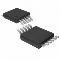
LTC2402CMS#TRPBF Linear Technology, LTC2402CMS#TRPBF Datasheet - Page 23

LTC2402CMS#TRPBF
Manufacturer Part Number
LTC2402CMS#TRPBF
Description
IC ADC 24BIT 2CH MICROPWR 10MSOP
Manufacturer
Linear Technology
Datasheet
1.LTC2401CMSPBF.pdf
(32 pages)
Specifications of LTC2402CMS#TRPBF
Number Of Bits
24
Sampling Rate (per Second)
7.5
Data Interface
MICROWIRE™, Serial, SPI™
Number Of Converters
2
Power Dissipation (max)
1mW
Voltage Supply Source
Single Supply
Operating Temperature
0°C ~ 70°C
Mounting Type
Surface Mount
Package / Case
10-TFSOP, 10-MSOP (0.118", 3.00mm Width)
Lead Free Status / RoHS Status
Lead free / RoHS Compliant
Available stocks
Company
Part Number
Manufacturer
Quantity
Price
APPLICATIO S I FOR ATIO
reference, on a regular FR-4 board, signal propagation
velocity is approximately 183ps/inch for internal traces
and 170ps/inch for surface traces. Thus, a driver gener-
ating a control signal with a minimum transition time of
1ns must be connected to the converter pin through a
trace shorter than 2.5 inches. This problem becomes
particularly difficult when shared control lines are used
and multiple reflections may occur. The solution is to
carefully terminate all transmission lines close to their
characteristic impedance.
Parallel termination near the LTC2401/LTC2402 pin will
eliminate this problem but will increase the driver power
dissipation. A series resistor between 27
placed near the driver or near the LTC2401/LTC2402 pin
will also eliminate this problem without additional power
dissipation. The actual resistor value depends upon the
trace impedance and connection topology.
Driving the Input and Reference
The analog input and reference of the typical delta-sigma
analog-to-digital converter are applied to a switched ca-
pacitor network. This network consists of capacitors
switching between the analog input (V
and FS
at both V
is shown in Figure 15.
The key to understanding the effects of this dynamic
input current is based on a simple first order RC time
constant model. Using the internal oscillator, the
Figure 15. LTC2401/LTC2402 Equivalent Analog Input Circuit
CH0/CH1
FS
ZS
SET
SET
I
IN
SET
IN
SWITCHING FREQUENCY
f = 153.6kHz FOR INTERNAL OSCILLATOR (f
f = f
V
(Pin 2). The result is small current spikes seen
CC
and V
EOSC
V
I
I
REF(LEAK)
REF(LEAK)
CC
FOR EXTERNAL OSCILLATORS
REF
I
I
IN(LEAK)
IN(LEAK)
U
. A simplified input equivalent circuit
R
R
R
U
5k
5k
5k
SW
SW
SW
W
24012 F15
I
IN
AVERAGE INPUT CURRENT:
O
= 0.25(V
= LOGIC LOW OR HIGH)
IN
), ZS
C
2.5pF (TYP)
EQ
IN
– 0.5 • V
SET
U
and 56
(Pin 5)
REF
)fC
EQ
LTC2401/LTC2402’s internal switched capacitor network
is clocked at 153,600Hz corresponding to a 6.5 s sam-
pling period. Fourteen time constants are required each
time a capacitor is switched in order to achieve 1ppm
settling accuracy.
Therefore, the equivalent time constant at V
should be less than 6.5 s/14 = 460ns in order to achieve
1ppm accuracy.
Input Current (V
If complete settling occurs on the input, conversion results
will be uneffected by the dynamic input current. If the
settling is incomplete, it does not degrade the linearity
performance of the device. It simply results in an offset/
full-scale shift, see Figure 16. To simplify the analysis of
input dynamic current, two separate cases are assumed:
large capacitance at V
tance at V
If the total capacitance at V
(< 0.01 F), relatively large external source resistances (up
to 20k for 20pF parasitic capacitance) can be tolerated
without any offset/full-scale error. Figures 18 and 19 show
a family of offset and full-scale error curves for various
small valued input capacitors (C
of input source resistance.
For large input capacitor values (C
spikes are averaged by the capacitor into a DC current. The
gain shift becomes a linear function of input source
TUE
ZS
SET
IN
(C
Figure 16. Offset/Full-Scale Shift
IN
IN
< 0.01 F).
)
IN
LTC2401/LTC2402
(C
IN
V
IN
> 0.01 F) and small capaci-
IN
(see Figure 17) is small
IN
< 0.01 F) as a function
IN
> 0.01 F), the input
IN
FS
24012 F16
and V
SET
23
REF


