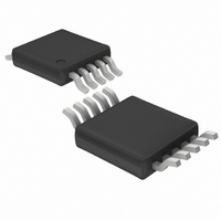
LTC2411IMS#TRPBF Linear Technology, LTC2411IMS#TRPBF Datasheet - Page 38

LTC2411IMS#TRPBF
Manufacturer Part Number
LTC2411IMS#TRPBF
Description
IC A/D CONV 24BIT MICRPWR 10MSOP
Manufacturer
Linear Technology
Datasheet
1.LTC2411CMSPBF.pdf
(40 pages)
Specifications of LTC2411IMS#TRPBF
Number Of Bits
24
Sampling Rate (per Second)
7.5
Data Interface
MICROWIRE™, Serial, SPI™
Number Of Converters
2
Power Dissipation (max)
1mW
Voltage Supply Source
Single Supply
Operating Temperature
-40°C ~ 85°C
Mounting Type
Surface Mount
Package / Case
10-TFSOP, 10-MSOP (0.118", 3.00mm Width)
Lead Free Status / RoHS Status
Lead free / RoHS Compliant
Available stocks
Company
Part Number
Manufacturer
Quantity
Price
APPLICATIO S I FOR ATIO
LTC2411/LTC2411-1
gain error or due to offset voltages. A 1 V/ C offset voltage
drift translates into 0.05ppm/ C gain error. Simpler alter-
natives, with the amplifiers providing gain using resistor
arrays for feedback, can produce results that are similar to
bridge sensing schemes via attenuators. Note that the
amplifiers must have high open-loop gain or gain error will
be a source of error. The fact that input offset voltage has
relatively little effect on overall error may lead one to use
low performance amplifiers for this application. Note that
the gain of a device such as an LF156, (25V/mV over
temperature) will produce a worst-case error of –180ppm
at a noise gain of 3, such as would be encountered in an
inverting gain of 2, to produce –10V from a 5V reference.
The error associated with the 10V excitation would be
–80ppm. Hence, overall reference error could be as high
as 130ppm, the average of the two.
Figure 47 shows a similar scheme to provide excitation
using resistor arrays to produce precise gain. The circuit
is configured to provide 10V and –5V excitation to the
bridge, producing a common mode voltage at the input to
38
U
U
Figure 46. Use a Differential Multiplexer to Expand Channel Capability
TO OTHER
DEVICES
W
5V
U
12
14
15
11
1
5
2
4
74HC4052
8
16
9
10
the LTC2411/LTC2411-1 of 2.5V, maximizing the AC input
range for applications where induced 60Hz could reach
amplitudes up to 2V
The circuits in Figures 45 and 47 could be used where
multiple bridge circuits are involved and bridge output can
be multiplexed onto a single LTC2411/LTC2411-1, via an
inexpensive multiplexer such as the 74HC4052.
Figure 46 shows the use of an LTC2411/LTC2411-1 with
a differential multiplexer. This is an inexpensive multi-
plexer that will contribute some error due to leakage if
used directly with the output from the bridge, or if resistors
are inserted as a protection mechanism from overvoltage.
Although the bridge output may be within the input range
of the A/D and multiplexer in normal operation, some
thought should be given to fault conditions that could
result in full excitation voltage at the inputs to the multi-
plexer or ADC. The use of amplification prior to the
multiplexer will largely eliminate errors associated with
channel leakage developing error voltages in the source
impedance.
13
3
6
+
47 F
2
3
4
5
REF
REF
IN
IN
LTC2411-1
+
–
LTC2411/
+
–
GND
V
5V
CC
6
1
RMS
.
2411 F46
A0
A1


