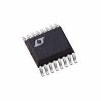
LTC2413IGN#TRPBF Linear Technology, LTC2413IGN#TRPBF Datasheet - Page 14

LTC2413IGN#TRPBF
Manufacturer Part Number
LTC2413IGN#TRPBF
Description
IC A/D CONV 24BIT MICRPWR 16SSOP
Manufacturer
Linear Technology
Datasheet
1.LTC2413CGN.pdf
(44 pages)
Specifications of LTC2413IGN#TRPBF
Number Of Bits
24
Sampling Rate (per Second)
6.8
Data Interface
MICROWIRE™, Serial, SPI™
Number Of Converters
2
Power Dissipation (max)
1mW
Voltage Supply Source
Single Supply
Operating Temperature
-40°C ~ 85°C
Mounting Type
Surface Mount
Package / Case
16-SSOP (0.150", 3.90mm Width)
Lead Free Status / RoHS Status
Lead free / RoHS Compliant
Available stocks
Company
Part Number
Manufacturer
Quantity
Price
APPLICATIO S I FOR ATIO
LTC2413
on the rising edge of the 32nd SCK pulse. On the falling
edge of the 32nd SCK pulse, SDO goes HIGH indicating the
initiation of a new conversion cycle. This bit serves as EOC
(Bit 31) for the next conversion cycle. Table 2 summarizes
the output data format.
As long as the voltage on the IN
within the – 0.3V to (V
operating range, a conversion result is generated for any
differential input voltage V
+FS = 0.5 • V
+FS, the conversion result is clamped to the value corre-
sponding to the +FS + 1LSB. For differential input voltages
below –FS, the conversion result is clamped to the value
corresponding to –FS – 1LSB.
14
Table 2. LTC2413 Output Data Format
Differential Input Voltage
V
V
0.5 • V
0.25 • V
0.25 • V
0
–1LSB
– 0.25 • V
– 0.25 • V
– 0.5 • V
V
*The differential input voltage V
**The differential reference voltage V
IN
IN
IN
* 0.5 • V
* < –0.5 • V
*
REF
REF
REF
REF
REF
. For differential input voltages greater than
REF
REF
** – 1LSB
**
** – 1LSB
**
**
** – 1LSB
REF
U
REF
**
**
SDO
SCK
CS
CC
U
IN
Hi-Z
+ 0.3V) absolute maximum
SLEEP
from –FS = –0.5 • V
+
and IN
IN
BIT 31
EOC
= IN
W
Bit 31
1
EOC
REF
–
0
0
0
0
0
0
0
0
0
0
+
pins is maintained
– IN
BIT 30
= REF
“0”
–
.
2
+
Bit 30
DMY
– REF
Figure 3. Output Data Timing
0
0
0
0
0
0
0
0
0
0
BIT 29
U
SIG
3
–
.
REF
Bit 29
BIT 28
SIG
MSB
1
1
1
1
1
0
0
0
0
0
to
4
DATA OUTPUT
BIT 27
Bit 28
Simultaneous Frequency Rejection
The LTC2413 internal oscillator provides better than 87dB
normal mode rejection over the range of 49Hz to 61.2Hz as
shown in Figure 4. For this simultaneous 50Hz/60Hz
rejection, F
When a fundamental rejection frequency different from
the range 49Hz to 61.2Hz is required or when the converter
must be sychronized with an outside source, the LTC2413
can operate with an external conversion clock. The conveter
automatically detects the presence of an external clock
signal at the F
frequency f
2560Hz to be detected. The external clock signal duty cycle
is not significant as long as the minimum and maximum
specifications for the high and low periods, t
are observed.
MSB
1
0
0
0
0
1
1
1
1
0
5
Bit 27
26
0
1
1
0
0
1
1
0
0
1
O
EOSC
should be connected to GND.
LSB
O
BIT 5
pin and turns off the internal oscillator. The
24
27
Bit 26
of the external signal must be at least
0
1
0
1
0
1
0
1
0
1
BIT 0
32
Bit 25
0
1
0
1
0
1
0
1
0
1
CONVERSION
2413 F03
…
…
…
…
…
…
…
…
…
…
…
Bit 0
0
1
0
1
0
1
0
1
0
1
HEO
and t
sn2413 2413fs
LEO
,


