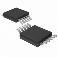
LTC2411-1IMS#TRPBF Linear Technology, LTC2411-1IMS#TRPBF Datasheet - Page 9

LTC2411-1IMS#TRPBF
Manufacturer Part Number
LTC2411-1IMS#TRPBF
Description
IC A/DCONV DIFF INPUT&REF 10MSOP
Manufacturer
Linear Technology
Datasheet
1.LTC2411CMSPBF.pdf
(40 pages)
Specifications of LTC2411-1IMS#TRPBF
Number Of Bits
24
Sampling Rate (per Second)
6.8
Data Interface
MICROWIRE™, Serial, SPI™
Number Of Converters
2
Power Dissipation (max)
1mW
Voltage Supply Source
Single Supply
Operating Temperature
-40°C ~ 85°C
Mounting Type
Surface Mount
Package / Case
10-TFSOP, 10-MSOP (0.118", 3.00mm Width)
Lead Free Status / RoHS Status
Lead free / RoHS Compliant
Available stocks
Company
Part Number
Manufacturer
Quantity
Price
V
(Pin 6) with a 10 F tantalum capacitor in parallel with
0.1 F ceramic capacitor as close to the part as possible.
REF
The voltage on these pins can have any value between GND
and V
more positive than the reference negative input, REF
at least 0.1V.
IN
voltage on these pins can have any value between
TYPICAL PERFOR A CE CHARACTERISTICS
PI FU CTIO S
CC
–100
–120
210
230
220
200
190
180
170
160
–20
–40
–60
–80
+
240
40
20
U
0
–45
+
(Pin 4), IN
(Pin 1): Positive Supply Voltage. Bypass to GND
Conversion Current
vs Temperature
0
Offset Error vs Output Data Rate
(Pin 2), REF
CC
F
CS = GND
SCK = NC
SDO = NC
V
REF
V
V
F
T
O
O
A
CC
INCM
IN
–30
10
= GND
= EXT OSC
= 25 C
OUTPUT DATA RATE (READINGS/SEC)
= 0V
as long as the reference positive input, REF
–
= 5V
= GND
U
= 2.5V
20
–15
30
TEMPERATURE ( C)
0
–
40
(Pin 5): Differential Analog Input. The
15
–
50
(Pin 3): Differential Reference Input.
U
V
30
REF
60
V
V
V
V
V
REF
CC
CC
= 2.5V
45
CC
CC
70
= 5.5V
= 2.7V
= 5V
= 5V
= 3V
W
60
80
75
2411 G25
90
2411 G28
U
100
90
650
600
550
500
450
400
350
300
250
200
150
22
21
20
19
18
0
0
Conversion Current
vs Output Data Rate
Resolution (NOISE
vs Output Data Rate
REF
REF
IN
IN
T
SCK = NC
SDO = NC
CS = GND
F
V
REF
V
V
F
RES = LOG
T
A
O
O
A
CC
INCM
IN
+
–
10
= 25 C
= EXT OSC
10
OUTPUT DATA RATE (READINGS/SEC)
= EXT OSC
= 25 C
OUTPUT DATA RATE (READINGS/SEC)
+
–
= GND
= GND
= 0V
–
= 5V
= V
= GND
= GND
= 2.5V
20
20
CC
–
+
, by
2
, is
30
(V
30
REF
40
40 50
/NOISE
V
V
REF
REF
50
GND – 0.3V and V
converter bipolar input range (V
from – 0.5 • (V
range, the converter produces unique overrange and
underrange output codes.
GND (Pin 6): Ground. Connect this pin to a ground plane
through a low impedance connection.
CS (Pin 7): Active LOW Digital Input. A LOW on this pin
enables the SDO digital output and wakes up the ADC.
Following each conversion the ADC automatically enters
V
V
= 2.5V
RMS
CC
= 5V
RMS
CC
60 70
60
= 5V
= 3V
)
70
1LSB)
80
80
90
90
2411 G26
2411 G29
100
100
REF
LTC2411/LTC2411-1
) to 0.5 • (V
CC
22
20
18
16
14
12
10
+ 0.3V. Within these limits, the
3
2
0
5
4
1
–45
0
Sleep Mode Current
vs Temperature
Resolution (INL
vs Output Data Rate
V
REF
V
V
F
RES = LOG
T
O
CC
INCM
IN
A
–30
10
= EXT OSC
= 25 C
OUTPUT DATA RATE (READINGS/SEC)
–
= 0V
= 5V
= GND
= 2.5V
20
–15
REF
IN
2
30
(V
TEMPERATURE ( C)
0
REF
= IN
). Outside this input
40
/INL
15
MAX
V
50
+
MAX
REF
30
– IN
)
60
= 2.5V
V
V
V
V
CC
CC
1LSB)
45
CC
CC
70
–
= 5.5V
= 2.7V
= 5V
= 3V
V
) extends
F
CS = V
SCK = NC
SDO = NC
60
REF
O
80
= GND
= 5V
75
2411 G27
90
CC
2411 G30
9
100
90


