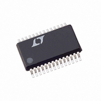
LTC2418CGN#TR Linear Technology, LTC2418CGN#TR Datasheet - Page 26

LTC2418CGN#TR
Manufacturer Part Number
LTC2418CGN#TR
Description
IC ADC 24BIT DIFF INPUT 28SSOP
Manufacturer
Linear Technology
Datasheet
1.LTC2418CGNPBF.pdf
(48 pages)
Specifications of LTC2418CGN#TR
Number Of Bits
24
Sampling Rate (per Second)
7.5
Data Interface
MICROWIRE™, Serial, SPI™
Number Of Converters
1
Power Dissipation (max)
1mW
Voltage Supply Source
Single Supply
Operating Temperature
0°C ~ 70°C
Mounting Type
Surface Mount
Package / Case
28-SSOP (0.150", 3.95mm Width)
Lead Free Status / RoHS Status
Contains lead / RoHS non-compliant
Other names
LTC2418CGNTR
Available stocks
Company
Part Number
Manufacturer
Quantity
Price
LTC2414/LTC2418
APPLICATIO S I FOR ATIO
Input Current
If complete settling occurs on the input, conversion re-
sults will be unaffected by the dynamic input current. An
incomplete settling of the input signal sampling process
may result in gain and offset errors, but it will not degrade
the INL performance of the converter. Figure 11 shows the
mathematical expressions for the average bias currents
flowing through the IN
sampling charge transfers when integrated over a sub-
stantial time period (longer than 64 internal clock cycles).
The effect of this input dynamic current can be analyzed
using the test circuit of Figure 12. The C
includes the LTC2414/LTC2418 pin capacitance (5pF typi-
cal) plus the capacitance of the test fixture used to obtain
the results shown in Figures 13 and 14. A careful imple-
mentation can bring the total input capacitance (C
C
than the one predicted by Figures 13 and 14. For simplic-
ity, two distinct situations can be considered.
For relatively small values of input capacitance (C
0.01µF), the voltage on the sampling capacitor settles
almost completely and relatively large values for the
26
PAR
) closer to 5pF thus achieving better performance
SWITCHING FREQUENCY
f
f
SW
SW
V
V
I
V
V
I
REF
REF
I
I
REF
REF
IN
IN
IN
IN
= 76800Hz INTERNAL OSCILLATOR (F
= 0.5 • f
+
+
–
–
+
+
–
–
V
V
EOSC
CC
CC
V
V
EXTERNAL OSCILLATOR
I
I
I
I
U
LEAK
LEAK
LEAK
LEAK
CC
CC
+
I
I
I
I
LEAK
LEAK
LEAK
LEAK
and IN
U
R
R
R
R
SW
SW
SW
SW
20k
20k
20k
20k
(TYP)
(TYP)
(TYP)
(TYP)
–
Figure 11. LTC2414/LTC2418 Equivalent Analog Input Circuit
pins as a result of the
O
W
= LOW OR HIGH)
2414/18 F11
PAR
U
C
18pF
(TYP)
capacitor
EQ
IN
IN
+
<
source impedance result in only small errors. Such values
for C
performance without significant benefits of signal filtering
and the user is advised to avoid them. Nevertheless, when
small values of C
of input multiplexers, wires, connectors or sensors, the
LTC2414/LTC2418 can maintain its exceptional accuracy
while operating with relative large values of source resis-
tance as shown in Figures 13 and 14. These measured
results may be slightly different from the first order
approximation suggested earlier because they include the
effect of the actual second order input network together
with the nonlinear settling process of the input amplifiers.
For small C
almost independently and there is little benefit in trying to
match the source impedance for the two pins.
Larger values of input capacitors (C
required in certain configurations for antialiasing or gen-
eral input signal filtering. Such capacitors will average the
input sampling charge and the external source resistance
will see a quasi constant input differential impedance.
When F
I IN
I IN
I REF
I REF
where
V
V
V
V
R
R
R
( )
( )
( )
( )
IN
INCM
REF
REFCM
EQ
EQ
EQ
IN
+
−
=
=
=
=
=
+
O
−
IN
AVG
AVG
: :
=
3 61
4 32
(
will deteriorate the converter offset and gain
REF
0 555 10
AVG
AVG
=
+
.
.
= LOW (internal oscillator and 60Hz notch), the
⎛
⎜
⎝
.
⎛
⎜
⎝
−
IN
=
=
M
IN
M
REF
+
IN
=
V
=
+
−
Ω
Ω
IN
−
•
values, the settling on IN
−
V
1 5
−
2
−
IN
REF
.
+
INTERNAL OSCILLATOR
+
1 5
IN
INTERNAL OSCILLATOR
.
+
2
12
V
+
•
IN
0 5
−
INCM
0 5
V
REF
•
−
.
V
⎞
⎟
⎠
)
REF
INCM
.
are unavoidably present as parasitics
V
/
•
REF
f
•
EOSC
R
0 5
−
−
R
−
0 5
EQ
.
⎞
⎟
⎠
EQ
.
V
−
−
V
•
REFCM
INCM
V
EXTERNAL OSCILLATOR
V
•
R
REFCM
INCM
R
EQ
EQ
+
+
V
REFCM
V
REFCM
60
50
IN
−
Hz Notch F
Hz Notch F
+
V
> 0.01µF) may be
REF
+
V
REF
and IN
V
IN
•
2
V
R
IN
•
2
EQ
R
(
(
EQ
O
O
–
=
=
occurs
LOW
HIGH
241418fa
)
)


