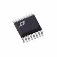
LTC1417ACGN Linear Technology, LTC1417ACGN Datasheet - Page 9

LTC1417ACGN
Manufacturer Part Number
LTC1417ACGN
Description
IC A/D CONV 14BIT SAMPLNG 16SSOP
Manufacturer
Linear Technology
Datasheet
1.LTC1417CGNPBF.pdf
(32 pages)
Specifications of LTC1417ACGN
Number Of Bits
14
Sampling Rate (per Second)
400k
Data Interface
MICROWIRE™, Serial, SPI™
Number Of Converters
1
Power Dissipation (max)
27.5mW Unipolar; 44mW Bipolar
Voltage Supply Source
Dual ±
Operating Temperature
0°C ~ 70°C
Mounting Type
Surface Mount
Package / Case
16-SSOP (0.150", 3.90mm Width)
Lead Free Status / RoHS Status
Contains lead / RoHS non-compliant
Available stocks
Company
Part Number
Manufacturer
Quantity
Price
Company:
Part Number:
LTC1417ACGN
Manufacturer:
LT
Quantity:
10 000
Part Number:
LTC1417ACGN
Manufacturer:
LTNEAR
Quantity:
20 000
Company:
Part Number:
LTC1417ACGN#PBF
Manufacturer:
CYPRESS
Quantity:
120
Part Number:
LTC1417ACGN#PBF
Manufacturer:
LINEAR/凌特
Quantity:
20 000
Company:
Part Number:
LTC1417ACGN#TRPBF
Manufacturer:
LT
Quantity:
450
APPLICATIONS
CONVERSION DETAILS
The LTC1417 uses a successive approximation algorithm
and an internal sample-and-hold circuit to convert an
analog signal to a 14-bit serial output. The ADC is com-
plete with a precision reference and an internal clock. The
control logic provides easy interface to microprocessors
and DSPs (please refer to Digital Interface section for the
data format).
Conversion start is controlled by the CONVST input. At the
start of the conversion, the successive approximation
register (SAR) is reset. Once a conversion cycle has
begun, it cannot be restarted.
During the conversion, the internal differential 14-bit
capacitive DAC output is sequenced by the SAR from the
most significant bit (MSB) to the least significant bit (LSB).
Referring to Figure 1, the A
nected to the sample-and-hold capacitors (C
ing the acquire phase and the comparator offset is nulled by
the zeroing switches. In this acquire phase, a minimum
delay of 500ns will provide enough time for the sample-
and-hold capacitors to acquire the analog signal. During
the convert phase, the comparator zeroing switches open,
placing the comparator in compare mode. The input
switches connect the C
transferring the differential analog input charge onto the
A
A
IN
IN
+
–
SAMPLE
SAMPLE
V
Figure 1. Simplified Block Diagram
DAC
+
V
HOLD
HOLD
DAC
U
–
C
C
SAMPLE
SAMPLE
C
C
DAC
DAC
+
–
INFORMATION
SAMPLE
+
–
U
SAR
IN
+
ZEROING SWITCHES
and A
+
–
capacitors to ground,
14
COMP
W
HOLD
HOLD
IN
REGISTER
–
SHIFT
inputs are con-
SAMPLE
U
1417 F01
) dur-
D
OUT
summing junction. This input charge is successively
compared with the binary weighted charges supplied by
the differential capacitive DAC. Bit decisions are made by
the high speed comparator. At the end of a conversion, the
differential DAC output balances the A
charges. The SAR contents (a 14-bit data word) that
represent the difference of A
through the serial pin D
DC Performance
One way of measuring the transition noise associated with
a high resolution ADC is to use a technique where a DC
signal is applied to the input of the ADC and the resulting
output codes are collected over a large number of conver-
sions. For example in Figure 2, the distribution of output
code is shown for a DC input that has been digitized 4096
times. The distribution is Gaussian and the RMS code
transition is about 0.33LSB.
DYNAMIC PERFORMANCE
The LTC1417 has excellent high speed sampling capabil-
ity. FFT (Fast Fourier Transform) test techniques are used
to test the ADC’s frequency response, distortion and
noise performance at the rated throughput. By applying
a low distortion sine wave and analyzing the digital output
using an FFT algorithm, the ADC’s spectral content can be
examined for frequencies beyond the fundamental.
Figure 3 shows a typical LTC1417 FFT plot.
3500
3000
2000
1500
1000
4000
2500
Figure 2. Histogram for 4096 Conversions
500
0
–2
–1
OUT
CODE
.
0
IN
+
1
and A
IN
2
1417 F02
+
LTC1417
IN
and A
–
are output
sn1417 1417fas
IN
–
input
9


