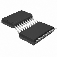
LTC1099CSW Linear Technology, LTC1099CSW Datasheet - Page 8

LTC1099CSW
Manufacturer Part Number
LTC1099CSW
Description
IC A/D CONV 8BIT HI-SPEED 20SOIC
Manufacturer
Linear Technology
Datasheet
1.LTC1099CNPBF.pdf
(16 pages)
Specifications of LTC1099CSW
Number Of Bits
8
Sampling Rate (per Second)
400k
Data Interface
Parallel
Number Of Converters
3
Power Dissipation (max)
55mW
Voltage Supply Source
Single Supply
Operating Temperature
0°C ~ 70°C
Mounting Type
Surface Mount
Package / Case
20-SOIC (0.300", 7.50mm Width)
Lead Free Status / RoHS Status
Contains lead / RoHS non-compliant
Other names
LTC1099CS
Available stocks
Company
Part Number
Manufacturer
Quantity
Price
Part Number:
LTC1099CSW
Manufacturer:
LINEAR/凌特
Quantity:
20 000
LTC1099
FUNCTIONAL DESCRIPTIO
also that variations in the bias voltage with time and
temperature will also be rejected. In this state, C1 charges
to V
The next step is the first comparison — the MS-Flash. T
and T+ are opened and T
comparator is:
There are 16 identical comparators each tied to the tap on
a 16 resistor ladder. The MS tap voltages vary from V
to 0V in 16 equal steps of V
Notice that capacitor C2 adds 0.5LSB to V
the converter transfer function by 0.5LSB, equally distrib-
uting the 1LSB quantization error to 0.5LSB.
The outputs of the 16 comparators are temporarily latched
and drive the 4-bit DAC directly without need of decoding.
8
STROBE
V
U
IN
IN
T
T
T+
T
. When T
–1
–2
Z
+ 0.5LSB – MS
SAMPLE
U
Z
opens, V
TAP
–1
IN
= 0V
is closed. The equation for each
is held on C1.
REF
MS TAP
0.5 LSB
LS TAP
/16.
DAC
V
0V
IN
(+)
(–)
(–)
(+)
(–)
(–)
Figure 6. Six Input Switched Capacitor Comparator
T+
U
IN
T
. This offsets
–1
T
–2
REF
C1
C2
Z
C1 = C2
HOLD
GROUND
VIRTUAL
This holds the DAC output constant for the next step — the
LS conversion. The LS conversion is started when T
opened and T
DAC approximation from V
charge to the virtual ground node. The equation for each
comparator is:
The 4-bit DAC approximation is input to all 16 compara-
tors. The LS tap voltages are converted to charge by
capacitor C2. LS taps vary from V
steps of V
on the virtual ground node to perform the LS-Flash con-
version. When this conversion is complete, the four LSBs
along with the four MSBs are transferred to the output
latches. In this way, all eight outputs will change
simultaneously.
V
T
Z
IN
+ 0.5LSB – V
REF
/256. The comparators look at the net charge
–2
is closed. Capacitor C1 subtracts the 4-bit
T
Z
DAC
– LS
IN
TAP
and inputs the difference
REF
= 0V
/16V to 0V in 16 equal
SAMPLE
1099 F06
–1
is


